Original Link: https://www.anandtech.com/show/14514/examining-intels-ice-lake-microarchitecture-and-sunny-cove
Examining Intel's Ice Lake Processors: Taking a Bite of the Sunny Cove Microarchitecture
by Dr. Ian Cutress on July 30, 2019 9:30 AM EST- Posted in
- CPUs
- Intel
- 10nm
- Microarchitecture
- Ice Lake
- Project Athena
- Sunny Cove
- Gen11
Intel has been building up this year to its eventual release of its first widely available consumer 10nm Core processor, codenamed "Ice Lake". The new SoC has an improved CPU core, a lot more die area dedicated to graphics, and is designed to be found in premium notebooks from major partners by the end of 2019, just in time for Christmas. With the new CPU core, Sunny Cove, Intel is promoting a clock-for-clock 18% performance improvement over the original Skylake design, and its Gen11 graphics is the first 1 teraFLOP single SoC graphics design. Intel spent some time with us to talk about what’s new in Ice Lake, as well as the product's direction.
The Core of Core: 10th Gen Core
Intel’s first batch of 10nm Ice Lake processors are being given the official brand name of ‘Intel 10th Generation Core’, and will feature up to four cores with hyperthreading and up to 64 execution units of Gen11 graphics. The aim of this first round of parts will be the thin-and-light mobile market in the form of the Ice Lake-U and Ice Lake-Y processors. Intel uses these designation for anything from 5W to 28W TDP, which covers all the mobile ultra-premium devices.
The cores inside Ice Lake-U are based on the ‘Sunny Cove’ microarchitecture, and are a further extension of the overall Core microarchitecture design. The new core affords several security benefits towards Spectre and Meltdown, and Intel is promoting a very healthy 18% IPC increase from its Skylake microarchitecture, which was initially launched as a 6th Gen Core part in 2015 (more on this later).
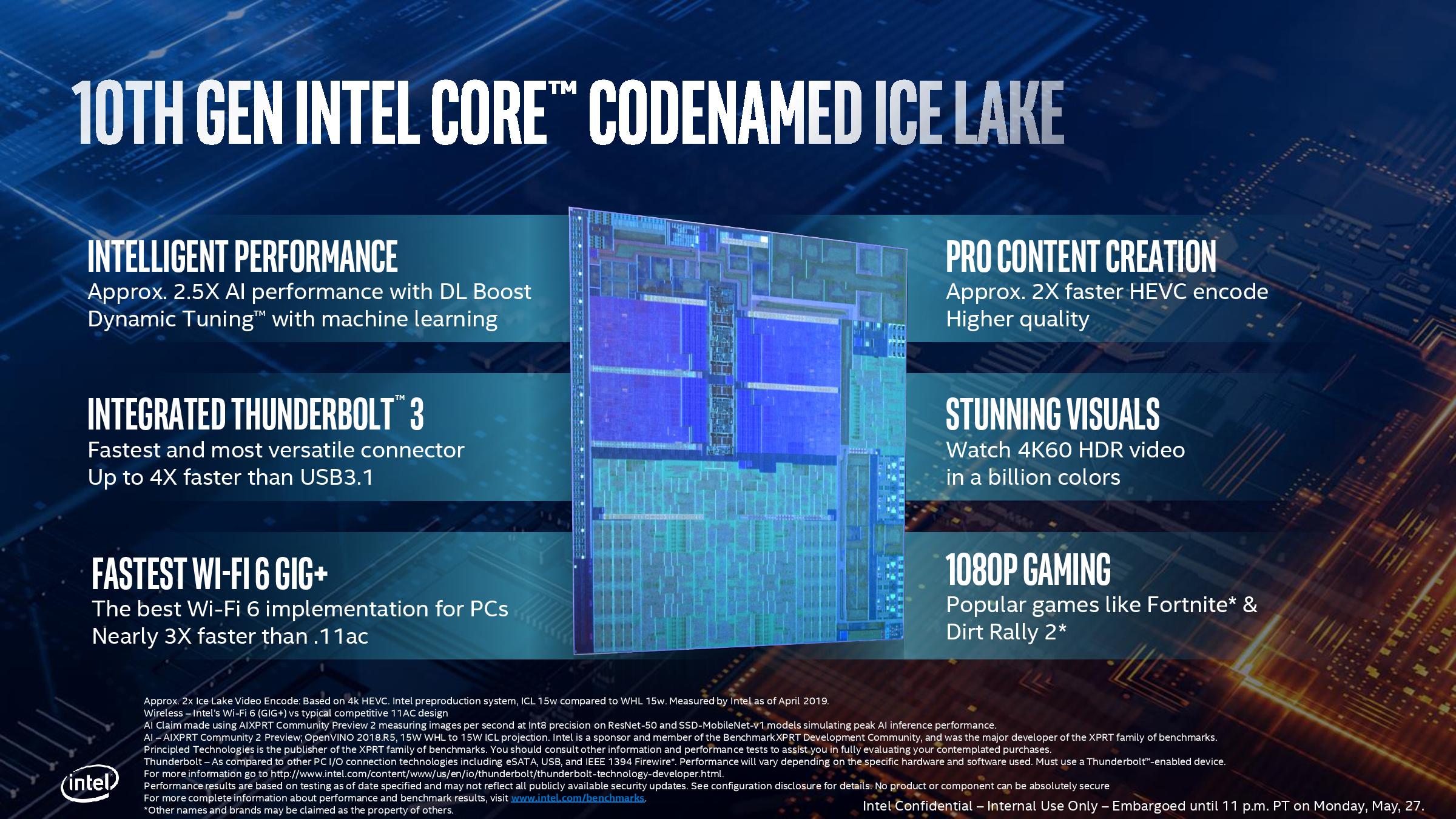
Asides from the core design, and the increased graphics performance, Intel is also putting a lot of effort into the rest of the design of the SoC. This includes AVX-512 extensions to help with deep learning and inference (applying pre-trained neural networks to new situations), integrated Thunderbolt 3 support for up to four full-bandwidth ports, CNVi support for Wi-Fi 6, and a range of platform designs under the umbrella of Intel’s new Project Athena initiative, which Intel hopes to spur on the next generation of premium devices and experiences in this market.
The Processors
Despite Intel continually talking about upcoming devices, and very general top down specifications, we have not seen a full, official CPU list from the company about what frequencies and what performance metrics the new Ice Lake processors will have. At an event a couple of months back, Intel showed this slide:
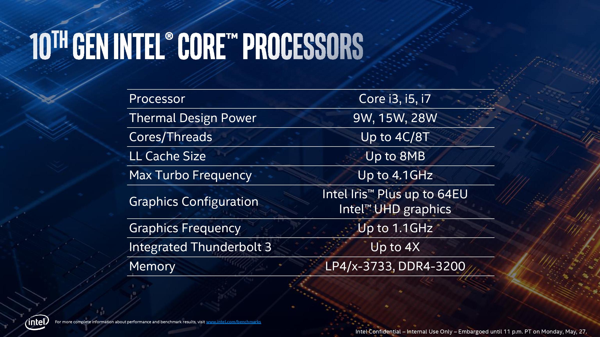
This slide states that we should expect to see i3, i5, and i7 versions of Ice Lake, with TDPs ranging from 9W to 28W, however the key value in there would be 15W. The processors will be up to four cores (so expect to see some dual cores), with a turbo frequency up to 4.1 GHz. Graphics will be available up to 64 execution units and up to 1.1 GHz, with certain platforms enabling four Thunderbolt 3 ports. Memory gets a healthy boost compared to previous platforms, with support being up to LPDDR4X-3733 (32 GB) or DDR4-3200 (64 GB). Each CPU has 16 PCIe 3.0 lanes for external use, although there are actually 32 in the design but 16 of these are tied up with Thunderbolt support.
Without a specific CPU list, it becomes a little worrying that the company hasn’t actually decided where the binning of these processors is going to fall. It also speaks to the fact that we are still several months away from having these processors in the market, so Intel is trying to find that balance of performance and yield. What we did discover at Computex earlier this year is that some vendors which are planning to have Ice Lake systems available, did disclose some CPU data:
There are of course some unconfirmed specification lists floating around the internet as well.
Ice Lake Design Wins, and Project Athena
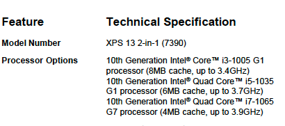
At Computex, Intel showed off a number of systems it says will be the leading designs for Ice Lake in Q4. These included a very impressive Dell XPS 13 system, a HP design with a wooden finish, and an Acer Swift model aiming to be the lightest Ice Lake laptop to come to market.
The Dell XPS 13
All of these devices come under Intel’s new Project Athena initiative.
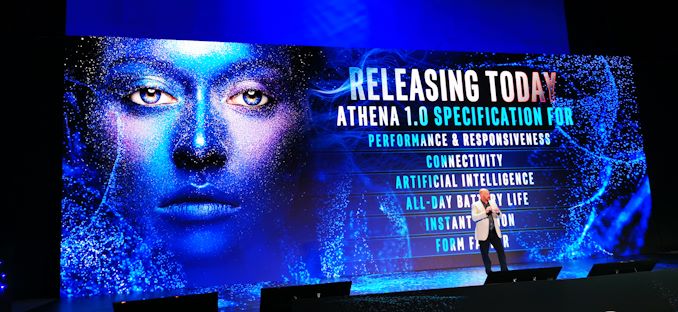
Project Athena borrows inspiration from Intel’s previous initiatives, such as Centrino and the Ultrabook. The goal here is to promote an ecosystem of Intel’s partners to design the next wave of devices and form factors that spurs on a good deal of innovation. This means that Project Athena has some very strict design targets that Intel’s partners have to follow and achieve in order to get the Athena designation/certification.

This means a lot of the following:
- Modern Connected Standby
- Biometric Login
- Wake from Sleep in <1 sec
- Core i5 or better
- >8GB DRAM in dual channel
- >256GB NVMe SSD, or Optane
- OpenVINO and WinML support
- 16+ hours of video playback
- 9+ hours of wireless web browsing
- Charge 4+hrs in 30 mins
- Thunderbolt 3, Wi-Fi 6, Gigabit LTE (optional)
- 2-in-1 or Clamshell,
- 12-15.6 inch, minimum resolution 1080p, touch display, narrow bezel on 3 sides
- Backlit keyboard, precision touchpad, pen support
Truth be told, supporting all of these means that the laptop should be a good buy with a decent user experience. These are a great set of goals to have for a mobile device, and it looks set that devices with the Athena designation should be very good.
However something to keep in mind is that in order to enable some of these technologies, it requires the OEMs to invest into Intel’s component ecosystem. Battery life, for example, helps if OEMs use the sub-1W panels that Intel has designated suitable for these devices. To implement Thunderbolt 3 and Wi-Fi 6 in a system is easy if a vendor uses an Ice Lake CPU, which also means that OEMs have to buy Intel’s AX200 chips (or a Killer AX1650, which is an AX200 underneath) to get Wi-Fi 6 to work. For Thunderbolt 3, re-timers are needed to support Type-C, and Intel makes those. The only other way to implement these features requires add-in cards which are higher power, and using those makes hitting the battery life targets, or the form factor requirements, difficult. Ultimately, to get the best of the Project Athena targets, the only way to do so is to buy more components from Intel or Intel approved component suppliers. Some may argue that programs like Project Athena end up cutting competition in this regard.
It should be noted that Ice Lake isn’t a requirement for Athena. But at this point it really, really, helps.
Intel will give the final Athena certification with a verification platform. This certification is built around what Intel says are ‘Key Experience Indicators’, such as the device being ready-to-go at a moment’s notice, providing enough worry-free battery life for common office tasks, and maintaining consistent responsiveness regardless of the state of the system.
Expect to see Athena devices in the market in Q4.
This Article
In this article, we’ll be going over Intel’s disclosures on Ice Lake, its new core Sunny Cove, as well as the new supported features and technologies within. We also comment on each of the new implemented items, with respect to user experience and realistic market/industry responses.
Combining 10nm CPU + 14nm Chipset
As with Intel’s previous low-power (sub 28W) mobile designs, the company will be combining the CPU and the chipset onto a single package. This typically helps in enabling a smaller motherboard design for thin and light systems that might want to dedicate that area to additional battery, or simply save the footprint altogether. The flip side is that there are more pin-outs, and the board design has to be suitable for the increased signal traces, but this is nothing new. For Ice Lake-U, Intel has stated that the CPU, which is being built on their second-generation 10nm "10+" process, will be paired with a new generation ‘14nm class’ chipset.
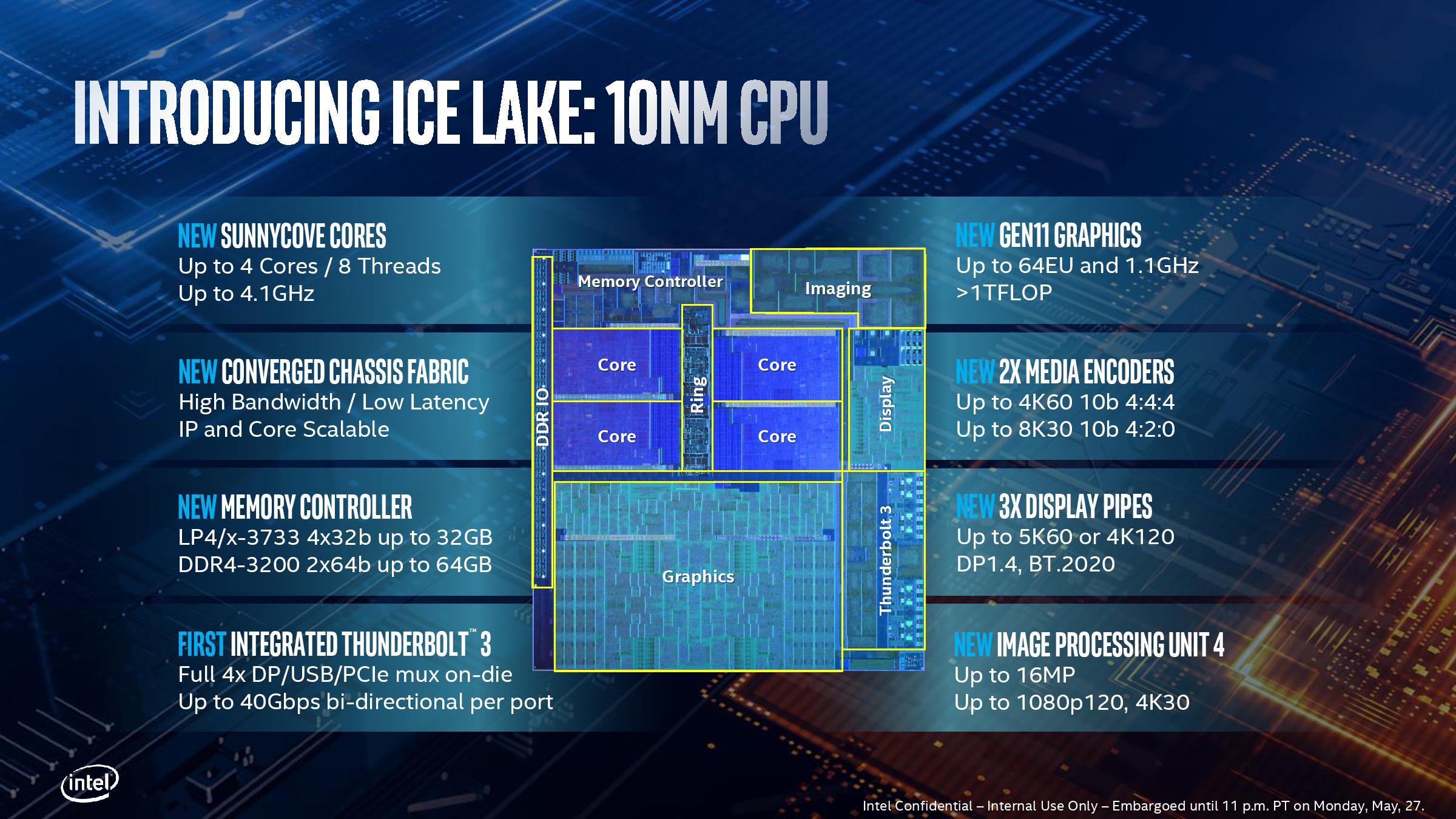
As stated on the previous page, the CPU will offer up to four cores, eight threads, go up to 4.1 GHz, provide integrated TB3 (more on that later), and a vast improvement to the graphics capabilities (also more on that later).
One of the big updates to the design will be enabling support for both DDR4 and LPDDR4/LPDDR4X on a single memory controller. Up until this point, only Intel’s latest Atom designs had LPDDR4 enabled, so this is a welcome addition to the main high-performance product line. In this instance Intel will support LPDDR4/X with up to four 32-bit channels at 3733 MT/s for 32 GB, or if a user needs more capacity, up to 64GB of DDR4-3200 with two 64-bit channels. The LPDDR4/X implementation will allow for lower idle power states, saving power and battery life when the memory is not in use, however it does this in exchange for maximum capacity. It’s an interesting tradeoff for sure. The peak power consumption of both modes in an equally populated system, given the respective frequency difference, should be similar.
One element that Intel hasn’t talked about is its ‘new converged chassis fabric’, which we believe to be a scalable power and environment control fabric that connects between chips in order to both transfer data but also to manage how and where power is applied within a system. The fact that Intel calls this ‘IP and Core scalable’ suggests that if vendors want to add additional supported chips to the system, say for example a future Intel AI chip, that might be possible and it could be controlled through this fabric. It will be interesting to see if Intel divulges any more of this information.
Not mentioned in this slide are the new performance enhancements, such as AVX-512 and other new instructions, which we’ll cover in detail a bit later.
The connection to the chipset is through a DMI 3.0 x4 link, as with current generations of Intel products.
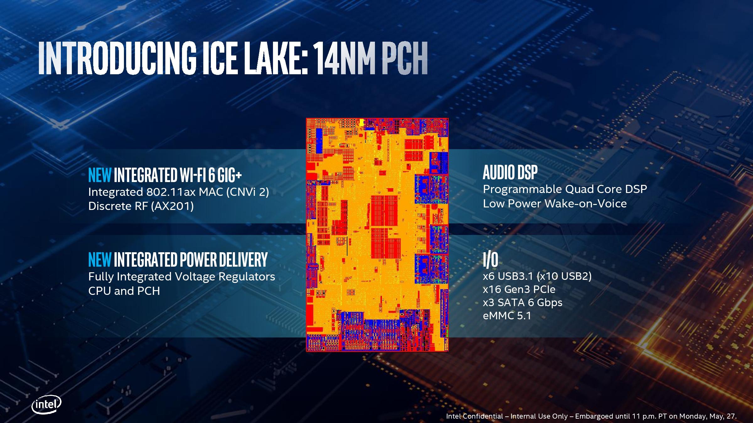
The new ‘14nm class’ chipset is also an update from Intel’s 8th Gen Core mobile processors. It does not yet have a series designation, but given the updates, this is likely to be a member of the 400-series chipset line.
With the new chipset, Intel has updated the proprietary CNVi protocol on the die to support CNVi 2, which is found on the latest Wi-Fi 6 Intel-Only RF modules, such as AX201. This update to a second generation implementation is likely to be for throughput reasons, given the increased bandwidth that Wi-Fi 6 provides over Wi-Fi 5.
Intel also promotes better integrated power delivery on the chipset, meaning that the PCH can share the same power rail as the CPU, reducing the number of on-board components inside the mobile system. This should reduce cost, and hopefully the thermal density of the power delivery onboard the chip doesn’t have a negative effect. Also on the power side, Intel states that the audio DSP on the chipset has also been improved for lower power operation.
On the IO side of the chipset, Ice Lake will support up to six ports of USB 3.1 (which is now USB 3.2 Gen 1 at 5 Gbps), or 10 USB 2.0 ports, or a mix. There are also 16 HSIO lanes which are broadly presented as PCIe 3.0, although given previous HSIO models it is likely that certain combinations of ports will be required for specific features. However this should afford at least two, if not three, potential PCIe 3.0 x4 NVMe drives in these systems. For SATA, there is access to three direct ports, but there is also an eMMC 5.1 link. Intel does not state if UFS is supported for super-small form factor systems.
Ice Lake is not Intel’s first crack at 10nm
We documented the history of Intel’s 10nm process with our review of the first 10nm CPU to come from the company. Our Core i3-8121U analysis of the Cannon Lake design is one Intel would rather forget – the manufacturing process didn’t yield, the frequency wasn’t there, the power consumption was too high, and the graphics were completely fused off. But hey, Intel still shipped it to customers by the end of 2017, and it found its way into some Chinese educational notebooks, and some NUCs, eventually, satisfying promises made to shareholders.

Fast forward almost 18 months, and we’re about to see Intel’s second take on 10nm with Ice Lake. Under Intel’s nomenclature, Ice Lake is technically being built with the ‘10+’ process, which is meant to be an improved version of the 10nm used in Cannon Lake. The fact that parts of the CPU are now working means that it earns that plus. Intel pointed to an extra metal layer (going from 12 to 13) in the manufacturing has helped with power delivery and frequency, and new transistor library designs and MIM caps have helped with voltages. Intel is also using a thin magnetic inductor array, and a recess in motherboard design for reduced package z-height.
As for Intel’s future, the company has stated at events that it is now developing future process nodes with these ‘BKM’ updates built into the lifecycle of the process node, such as 10+ and 10++ as part of the family of 10nm processes, and then beyond to 7nm with 7, 7+, and 7++ over the next few years. It’s worth noting that while Intel has officially shipped a first generation 10nm product, is promoting Ice Lake as a ‘10+’ second generation 10nm product, and has specified a number of 10nm class products up and down its product portfolio, we are still waiting on an official presentation about how Intel’s 10nm process works in a formal setting, rather than bits and pieces from events like ISSCC and IEDM. What we have pieced together from those events is likely out of date for 10+, however we do know that for 10nm Intel has three different libraries based on performance, each with different transistor densities: from 67 million transistors / mm2 for ultra-high performance, to 101 million transistors / mm2 for high-density logic. You can read more about it here.
Sunny Cove Microarchitecture: Going Deeper and Wider
Ice Lake falls under Intel’s ‘10th Gen Core’ family, and is based around the latest iteration of the ‘Core’ microarchitecture, which initially debuted over a decade ago and has received plenty of key critical enhancements and extra features along the way. Over the years we’ve seen improved prefetchers, smarter branch predictors, adjusted cache sizes and capabilities, deeper and wider execution, micro-op caches, accelerated calculation logic, and lower power operation, all designed to increase the instruction throughput, decrease cache misses, and improve power efficiency.
When Intel designs a new generation of Core, it tends to go in a lot of things: mobile CPUs, desktops, servers, sometimes embedded, new communications technologies, and plenty of other custom silicon besides. As a result, it has to scale, from low-end to high-end. One of Intel’s new Chief Architects, Jim Keller, says that Intel has a ‘milliwatt-to-megawatt’ strategy when it comes to product design, and it’s the Core microarchitecture that is currently bringing in the big $$$ to fund a lot of the R&D.
Before we go into the new Sunny Cove core, I should preface the explanations with a little warning. Intel’s previous microarchitecture update and design, Skylake, is Intel’s most profitable design ever. Part of that reason is that it has been around the block for four generations of products. Intel hasn’t changed the core in that time, for almost four years. At this point, we’ve been yearning for something that actually has changes. So please forgive a little excitement when covering a few of the more mundane updates.
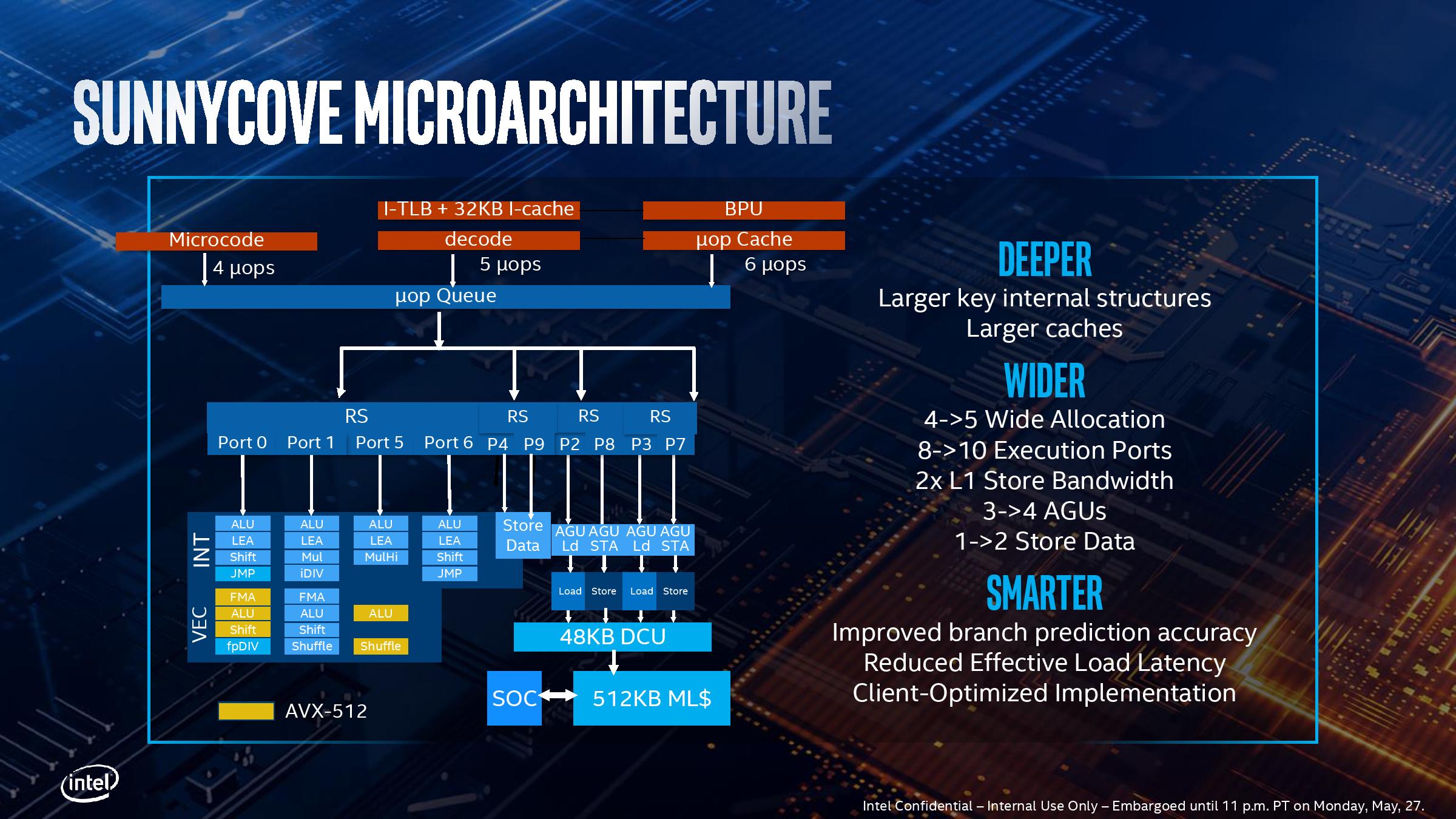
Sunny Cove Front End
Despite the instruction entry point into the core being at the front-end. Intel didn’t say too much about Sunny Cove in this respect. Typically Intel keeps the details of its prefetchers and branch predictors secret, although CPU Architect Ronak Singhal did state that it is by-and-large similar to the Skylake design. Ronak has said that the branch predictor has increased accuracy, and that the average/effective load latency has decreased, and by and large the front-end of the CPU has been optimized for client (read consumers/end-users), rather than servers, which Skylake was. The internal structures of the branch predictor unit and prefetcher are larger according to Intel, which should help improve accuracy.
The L1 instruction cache is still a 32 KiB 8-way design, and there are still five decoders in play. These decoders are split as one complex decoder and four simple decoders, and they can supply up to five micro-ops per cycle. There’s nothing drastically new in terms of op fusion we are told, just the general expected improvements, plus additional support for the new AVX-512 instructions.
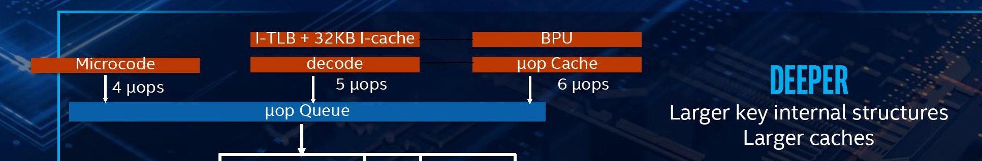
The micro-op cache gets an update here, from 1.5k entries to 2.25k entries. This is the first time that Intel has increased the micro-op cache size since Haswell, but it should be noted that the competition also has micro-op caches (ARM has 1.5k, AMD has 2k for Zen, 4k for Zen 2), and so refinement in this area is going to be critical. The micro-op cache can supply six micro-ops to the queue per cycle.
Overall, six micro-ops can be fed between the decoders/cache/direct micro-code per cycle. That is split between up to six per cycle from the cache, up to 5 from the decoders, and up to 4 from direct microcode (which gets fed through the complex decoder.
Out-of-Order Window
The micro-op queue, for rename/allocate/retire, has also increased. The design went from 182 micro-ops in Haswell to 224 in Skylake, but goes all the way up to 352 in Sunny Cove, a massive 57% increase. This will help managing which instructions are ready to be processed by the scheduler, although this often comes at the penalty of power. This is one of the advantages of using a smaller process node – there’s more power budget to go around, allowing a CPU team to design bigger queues.
| AnandTech | Haswell | Skylake | Sunny Cove |
| Reorder Buffer | 182 | 224 | 352 |
| In-Flight Stores | 72 | 72 | 128 |
| In-Flight Loads | 42 | 56 | 72 |
With the increased queue size, Intel also reports that support for in-flight loads and stores has increased: up from 72 loads in Skylake to 128 in Sunny Cove, and up from 56 stores in Skylake to 72 in Sunny Cove. This means that the in-flight load/store ratio is more weighted in favor of loads, which Intel states is part of the more user-focused design where loads end up being more important than stores.
Back End
This is where the fun happens. As with previous Intel designs over the years, we still have a unified scheduler for both integer and vector operations, however they are split between four different reservation stations depending on what operation is needed:
- One for four ALU ports, accepts 4 micro-ops/cycle
- One for two Store ports, accepts 2 micro-ops/cycle
- One for a pair of AGUs, one load, one store, accepts 2 micro-ops/cycle
- One for a pair of AGUs, one load, one store, accepts 2 micro-ops/cycle
In total, the number of execution ports has increased from 8 in Skylake to 10 in Sunny Cove. This allows for 10 micro-ops per cycle to be dispatched from the reorder buffer, a 25% increase. The two new ports lie in different areas: Skylake had 3 AGUs, supporting two loads and one store per cycle, but Sunny Cove now has 4 AGUs, for two loads and two stores per cycle. The other new port is a store data port. With these changes, the L1 data cache can now support two stores per cycle, effectively doubling the L1 store bandwidth.
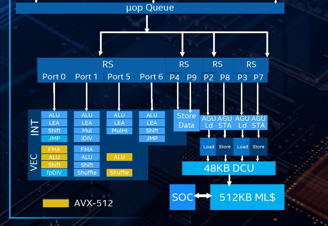
The L1 Data cache has increased, for the first time in over a decade. Intel has moved from a 32 KiB 8-way design up to a 48 KiB 12-way design, which should help reduce data cache misses significantly. This combined with the micro-op cache size increase is one of the easiest ways to reduce cache miss penalties. (For comparison, in Zen 2 AMD halved its L1-I size and doubled its micro-op cache, which it felt was a more efficient way of improving instruction throughput, but also the silicon area design had to be managed.)
Intel has also increased the L2 cache, up from 256 KiB to 512 KiB, and it is still non-inclusive of the L1 with a write-back policy. In order to assist the L2, the L2 TLB page table arrangement has also been improved, with up to 2k entries at 4K, 1k entries for 2M/4M (new, used to be shared with 4K), and up from 16 entries to 1024 entries at 1G. The cache improvements on Sunny Cove are certainly expected to work in Intel’s favor, especially when it comes to the enhanced graphics part of the design.
On a core-to-core level, Intel's recent designs have the following configurations:
| Microarchitecture Comparison | ||||||
| Skylake | Cannon Lake | Sunny Cove* | Zen | Zen 2 | ||
| L1-D Cache |
32 KiB/core 8-way |
32 KiB/core 8-way |
48 KiB/core 12-way |
32 KiB/core 8-way |
32 KiB/core 8-way |
|
| L1-I Cache |
32 KiB/core 8-way |
32 KiB/core 8-way |
32 KiB/core 8-way |
64 KiB/core 4-way |
32 KiB/core 8-way |
|
| L2 Cache |
256 KiB/core 4-way |
256 KiB/core 4-way |
512 KiB/core 8-way |
512 KiB/core 8-way |
512 KiB/core 8-way |
|
| L3 Cache |
2 MiB/core 16-way |
2 MiB/core 16-way |
2 MiB/core 16-way |
2 MiB/core | 4 MiB/core | |
| L3 Cache Type | Inclusive | Inclusive | Inclusive | Non-Inclusive | Non-Inclusive | |
| Decode | 4 + 1 | 4 + 1 | 4 + 1 | 4 | 4 | |
| uOP Cache | 1.5k | 1.5k | 2.25k | 2k | 4k | |
| Reorder Buffer | 224 | 224 | 352 | 192 | 224 | |
| Execution Ports | 8 | 8 | 10 | 10 | 11 | |
| AGUs | 2 + 1 | 2 + 1 | 2 + 2 | 1 + 1 | 2 + 1 | |
| AVX-512 | - | 1 x FMA | 1 x FMA | - | ||
| * Sunny Cove numbers for Client. Server will have different L2/L3 cache and FMA, like Skylake | ||||||
For the execution ports, now that Intel has moved AVX-512 into the mainstream Core design, there are a few changes. AVX-512 is now supported on Port 0 (FMA, ALU, Shift) and Port 5 (ALU, Shuffle). There is only one AVX-512 port, but also a 256-bit FMA port, so either 1x512-bit or 2x256-bit throughput is possible.
Overall the design allows for:
| Back-End Execution Resources | ||||||||
| Skylake | Port | Sunny Cove | ||||||
| Integer | ||||||||
| JMP | Shift | ALU | 0 | ALU | LEA | Shift | JMP | |
| LEA | ALU | 1 | ALU | LEA | Mul | iDIV | ||
| Mul | LEA | ALU | 5 | ALU | LEA | MulHi | ||
| JMP | Shift | ALU | 6 | ALU | LEA | Shift | JMP | |
| Vector / FP | ||||||||
| fpDIV | Shift | ALU | FMA | 0 | FMA | ALU | Shift | fpDIV |
| Shift | ALU | FMA | 1 | FMA | ALU | Shift | Shuffle | |
| Shuffle | ALU | FMA | 5 | FMA | ALU | Shuffle | ||
The parts highlighted in bold are different in the Sunny Cove core.
The TL;DR
The core improvements can be summed up as follows:
- Better prefetchers and branch predictors
- +50% L1 Data Cache
- +100% L1 Store Bandwidth
- +100% L2 Cache w/improved L2 TLB
- +50% Micro-op Cache
- +25% uops/cycle into reorder buffer
- +57% reorder buffer size
- +25% execution ports
- AVX-512 with VNNI
Add in better memory support (Up to LPDDR4X-3733) and better graphics (64 EUs of Gen11), and it’s a really nice update.
For all of this, Intel is promoting a +18% IPC increase over Skylake, which ranges from 0.98x to 1.40x depending on the workload (SPEC2006, SPEC2017, SYSMark 2014SE, WebXPRT, CineBench), or a +47% increase in real world tasks against Broadwell.

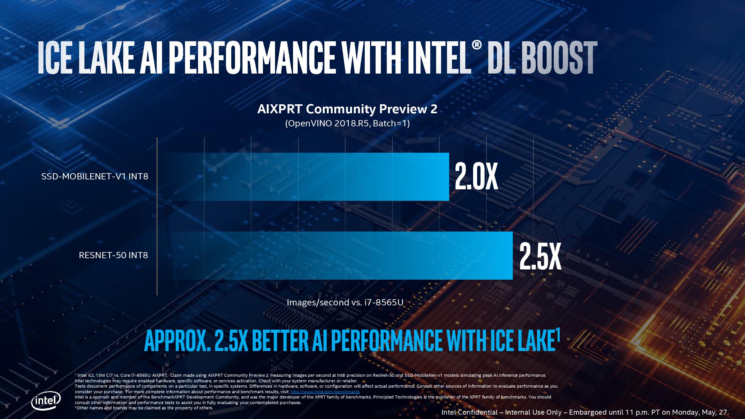
When AVX512 is in play, with DLBoost, Intel is promoting a 2.0x-2.5x increase against the best Whiskey Lake has to offer.
We’ll cover Intel’s claims later in the analysis.
Gen11 Graphics: Competing for 1080p Gaming
The new message from Intel is that it is driving to deliver deep gaming experiences with its technology, and the nod to the future is specifically what it wants to do with its graphics technology. Until the company is ready with its Xe designs for 2020 and beyond, it wants to start to lead the way with better integrated designs. That starts with Ice Lake, where the most powerful version of Ice Lake will offer over 1TF of compute performance, support higher resolution HEVC, better display pipes, an enhanced rasterizer, and support for Adaptive Sync.
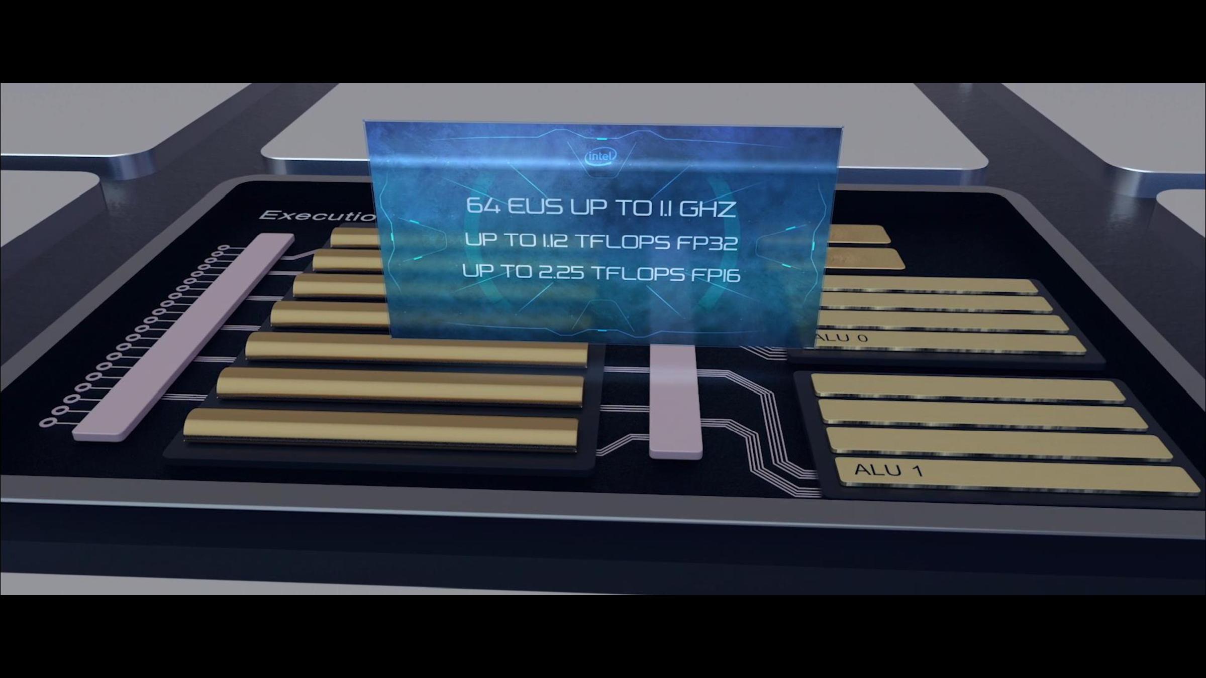
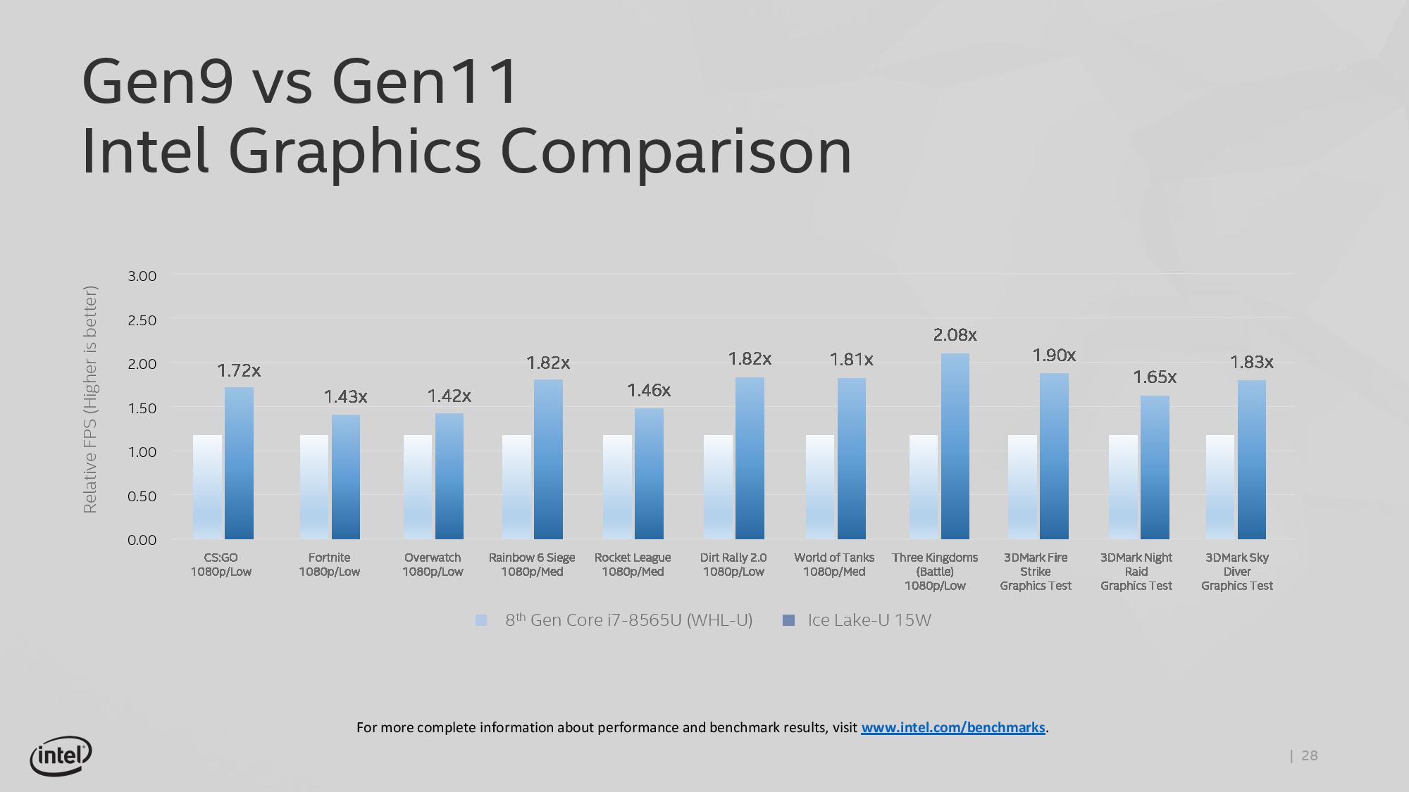
The key words in that last sentence were ‘the most powerful version’. Because Intel hasn’t really spoken about its product stack yet, the company has been leading with its most powerful Iris Plus designs. We assume this means 28W? That means its high-end performance products, in the best designs, with the fastest memory. Compared to the standard Gen9 implementation of 24 execution units at 1150 MHz turbo, the best Ice Lake Gen11 design will deliver 64 execution units up to a 1100 MHz frequency, good for 1.15 TF of FP32 performance, or 2.30 TF of FP16 performance. Intel promise up to 1.8x better frame rates in games with the best Ice Lake compared to an average 8th Gen Core (Kaby Lake) Gen9 implementation. Intel doesn’t compare the results to a hypothetical Cannon Lake Gen10 implementation.
Intel hasn’t stated how many graphics configurations it will offer, but there would appear to be several given what information has leaked out already. The high-end design with 64 execution units will be called Iris Plus, but there will be a ‘UHD’ version for mid-range and low-end parts, however Intel has not stated how many execution units these parts will have. We suspect that standard dividers will be in play, with 24/32/48 EU designs possible as different parts of the GPU are fused off. There may be some potential for increased frequency in these designs, reducing latency, but ultimately reduced performance over the top design.
It should be noted that Intel is promoting the top model as being suitable for 1080p low-to-mid gaming, which would imply that models with fewer execution units may struggle to hit those highs with different EU counts. Until Intel gives us a full and proper product list, it is hard to tell at this point.
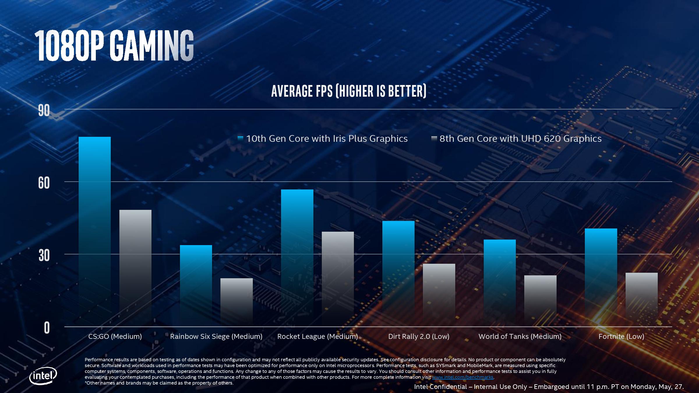
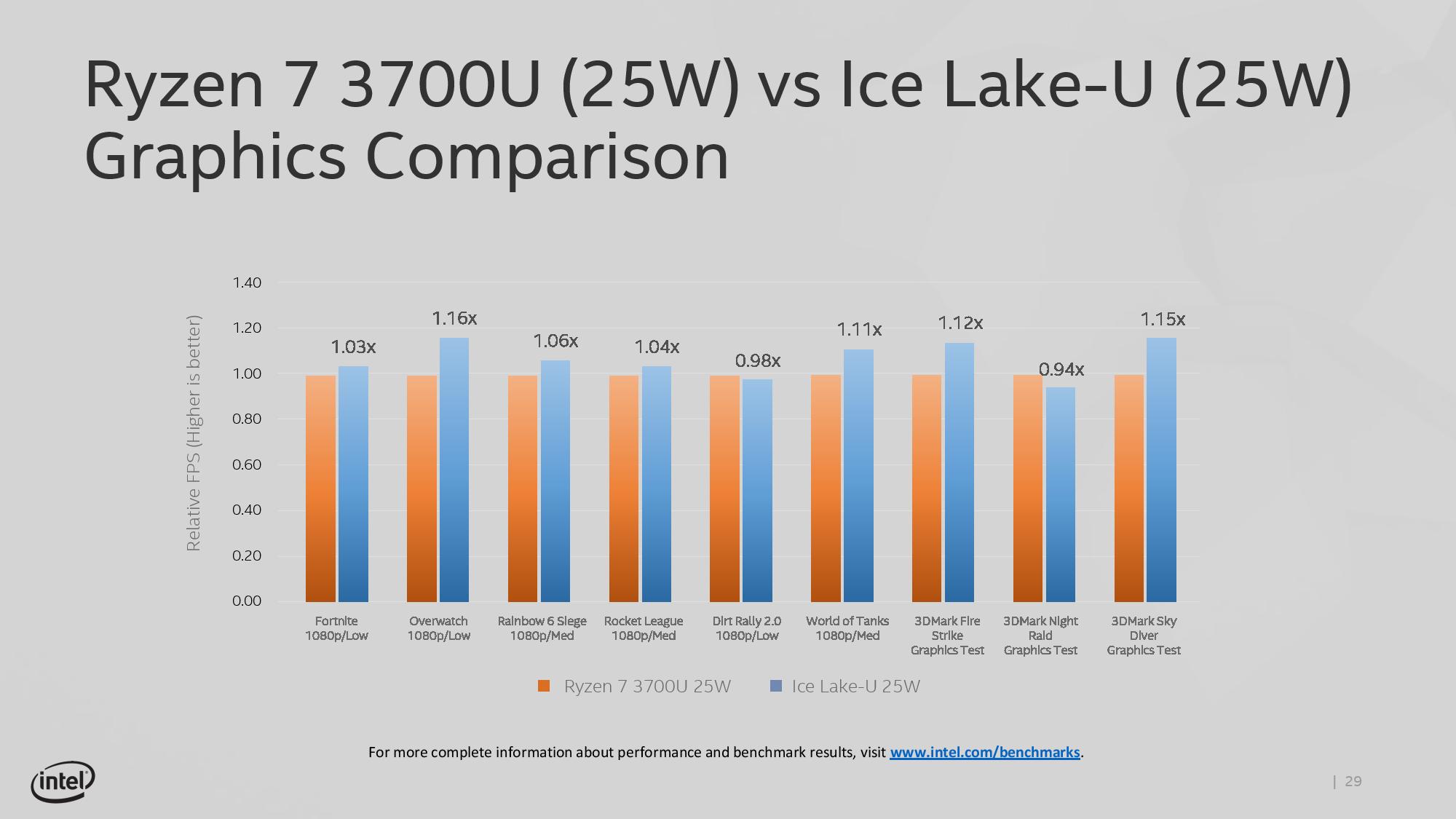
This slide, for example, shows where Intel expects its highest Ice Lake implementation to perform compared to the standard 8th Gen solution. As part of Computex, Intel also showed off some different data:
This graph shows relative FPS, rather than actual FPS, so it’s hard to see if certain games are just hitting 30 FPS in the highest mode. The results here are a function of the combination of increased EU count but also memory bandwidth.
Features for All
There are a number of features that all of the Gen11 graphics implementations will get, regardless of its number of execution units.
For its fixed function units, Gen11 supports two HEVC 10-bit encode pipelines, either two 4K60 4:4:4 streams simultaneously or one 8K30 4:2:2 stream using both pipelines at once. On display pipes, Gen11 has access to three 4K pipes split between DP1.4 HBR3 and HDMI 2.0b. There is also support for 2x 5K60 or 1x 4K120 with a 10-bit color depth.
The rasterizer gets an upgrade, and will now do 16 pixels per clock or 32 bilinear filtered texels per clock. Intel also gives some insight into the cache arrangements, with the execution units having their own 3 MiB of L3 cache and 0.5 MiB of shared local memory.
Intel recommends that to get the best out of the graphics, it should be paired with LPDDR4X-3733 memory in order to extract a healthy 50-60 GB/s bandwidth, and we should expect a number of Project Athena approved designs do just that. However, at the lower end of Ice Lake devices, we might see single channel DDR4 designs take over due to costs, which might limit performance. As always for integrated graphics, memory bandwidth is often a major bottleneck in performance. Back when Intel had eDRAM enabled Crystalwell designs, those chips were good for 50 GB/s bidirectional bandwidth, and we are almost at that stage with DRAM bandwidth designs now. It should be noted that there are tradeoffs with memory support: LPDDR4/X supports 4x 32b channels up to 32 GB with super low power consumption modes, but if users want more capacity, they’ll have to look to DDR4-3200 with 2x 64b channels up to 64 GB, but lose some performance and power savings.
Variable Rate Shading
A feature being implemented in Gen11 is Variable Rate Shading. VRS is a game-dependent technology that allows the GPU adjust the shading performance of the scene render based on what areas are important. All games currently do shading on a per-pixel basis, meaning that each pixel has a full calculation and that data is transferred to the final image. With VRS, shading is calculated over several pixels at once – essentially doing pixel shading in a coarser, lower-resolution manner – to save post-processing time by using averaged data.
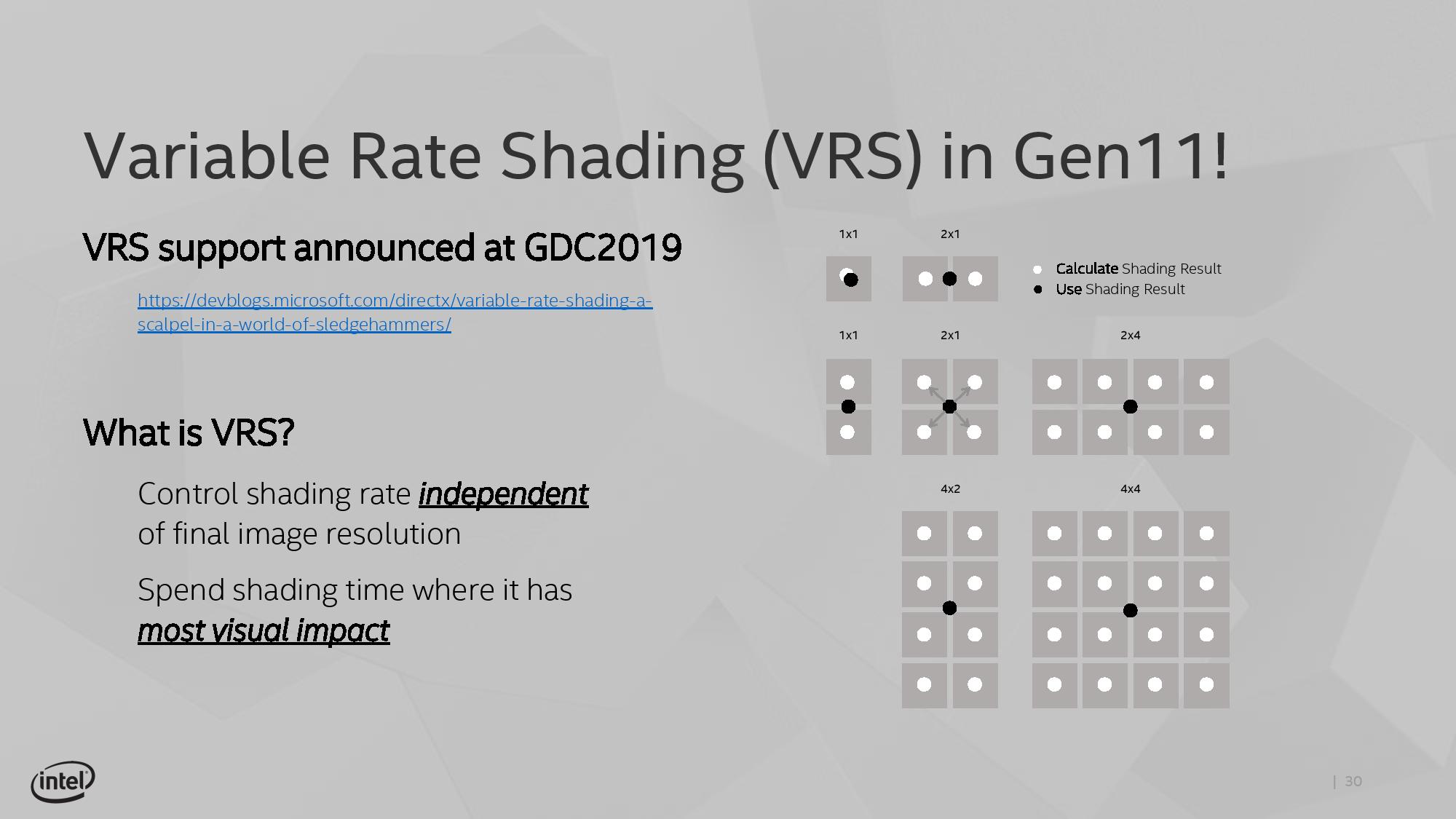
The idea is that using this method can reduce some of the load on the execution units, ultimately increasing the frame rate. The size of that combination of pixels can be adjusted on a per-frame basis as well, allowing the game to take advantage of processing budget where it exists, or pull back to a point where performance is needed. Ultimately Intel believes that any image quality loss is not noticeable, especially for the performance impact they expect it to provide. Intel states that this technology is useful for areas such as lighting adjustments, partially obscured objects (by fog/clouds), and areas that undergo blur, or foveated rendering – basically any area where clarity isn’t explicitly required to begin with.
The only issue here though is an ecosystem one – it requires the game developer support. Intel is already working with Epic to add it to the Unreal Engine, and Intel has worked with developers to enable support in titles such as Civilization 6. The difference in performance, according to Intel, can be up to a 30% FPS increase in a best-case scenario. NVIDIA already supports VRS through dedicated hardware, whereas AMD’s current solutions are best described as a more limited shader-based approximation.
DL Boost and New Instructions: Intel’s AI Acceleration Attack
If you like buzzwords, then the field of artificial intelligence is full of them. Unless you are deeply embedded in the use or development of the technologies in this field, it can be pretty easy to be overwhelmed by all the acronyms and how they relate to each other. This complication is multiplied out by the new technologies that hardware manufacturers develop in order to support the methods the expert’s use, especially as those methods transition from software implementations to hardware accelerated methods.
Intel’s side of the equation on this is two-fold. On one level, the company wants to accelerate how these algorithms are trained – Intel wants to be able to provide the raw horsepower and bandwidth to push millions of results to train these algorithms in order to improve accuracy and efficiency. Training on this scale typically happens at the datacenter, and Intel will happily promote its FPGAs or Neural Network Processors to help do this.
The other side of the discussion is inference – the art of taking those trained algorithms and showing them new data to make accurate predictions. The simple example of inference is showing an algorithm that has been trained to identify different objects a new image that it has never seen before. Inference, in contrast to training, happens at the device level, is less computationally strenuous, but can be optimized to a super low power hardware accelerated implementation. There can also be a tradeoff between speed/power and accuracy. Again, the most obvious example of this is a smartphone identifying that the camera is pointed at food, or a sunset, or a building, or a cat.
The two sides of artificial intelligence, training and inference, happen at very different ends of the spectrum. Training occurs at the application developer level, while inference happens very much at the user level. For products that ultimately end up in the hands of end-users, being able to accelerate inference is a key to user experience.
However, Intel has a problem here. In fact, all companies that sell mobile PC products to end-users have a problem. The concepts of interference, such as identifying an item on a camera view screen, are easy to understand in a smartphone form factor. But apply that logic to a laptop, a notebook, or a desktop, and the applicability of how AI can improve the user experience starts to get a little distorted. It is not immediately obvious in what ways that AI can improve what a user does on these devices. The smartphone, by contrast, is an easier sell.
As a result, Intel has needed to go out into the community. Its new chip, Ice Lake, is a sledgehammer, and it’s looking for a nail, no matter how small. The truth of it is that a lot of end-user software does not have artificial intelligence built into it – any ‘intelligence’ that most software has is typically a bunch of ‘if this then that’ statements which do not fall in this category.
This ‘hammer looking for a nail’ implementation was very apparent at Computex 2019. Intel showcased a few demos with its new technology, however most of them were fairly niche. Two examples of this include:
- Photo Album sorting: searching for all ‘beach’ photos in a photo album that hasn’t been manually tagged.
- Converting a single 2D image into a 3D model for use in 3D visualization environments
The first case might be interesting to the wider public – and indeed Apple already does something like this on macOS – however the second use case is currently aimed at business or archival use, which is a specific niche. Ultimately Intel is looking to increase the amount of available tools, even if they are niche, which can be accelerated on Ice Lake. Intel is taking all suggestions on this.
How Intel is accelerating these inference models is through its ‘DL Boost’ technology, which is essentially a form of vector acceleration.
DL Boost and AVX-512
One of the features of the Ice Lake cores is that silicon is dedicated to AVX-512 operation. This allows for 512-bit instructions and math to be executed at once. With Ice Lake, it marks the first consumer platform from Intel to support the feature, if you exclude Cannon Lake which was not widely available. To date only Intel’s Xeon Skylake or newer silicon, or Xeon Phi, has had AVX-512 as part of the design. As we saw in our review of Cannon Lake, when AVX-512 code is run on these systems, it can be very effective: a dual core system with AVX-512 outscored a 16-core system running AVX2 (AVX-256).
AVX-512 forms the basis for Intel’s DL Boost libraries, which form part of several SDKs in Intel’s software strategy, such as the OpenVINO toolkit. DL Boost takes advantage of the new core’s abilities to reform neural network calculations in the form of lower precision calculations, from FP32 to FP16 to INT8 and even down to INT2. The balance here is between accuracy, power, and computational complexity: for example, in most non-critical situations, dropping the accuracy of an inference calculation from 94% to 93% accuracy would be worth it if it reduced latency and power consumption by half. DL Boost accelerated libraries also allow for mathematical numerical transforms in neural network calculations to further increase throughput and decrease power.

Ultimately DL Boost covers the gamut from training to inference – Intel promotes its use on the server Xeon product line for training, whereas the Ice Lake consumer line of products will be focused on inference. Again, its usefulness when it comes to consumer products will initially be limited, given the lack of common AI inference workloads on modern systems. Intel promotes the AIXPRT synthetic benchmark suite as an example of performance uplift, however that focuses almost entirely on image recognition.
New Instructions
Alongside DL Boost, Intel has implemented a series of AVX-512 instructions for other use cases.
AVX-512_VBMI is one layer of Vector Byte Manipulation Instructions, which includes permutes and shifts:
- VPERMB: 64-byte any-to-any shuffle, 3 clocks, 1 per clock
- VPERMI2B: 128-byte any-to-any overwriting indexes, 5 clocks, 1 per 2 clocks
- VPERMT2B: 128-byte any-to-any overwriting tables, 5 clocks, 1 per 2 clocks
- VPMULTISHIFTQB: Base64 conversion, 3 clocks, 1 per clock
AVX-512_VBMI2 takes this a stage further, enabling expand and compress functionality
- VPCOMPRESSB: Store sparse packed byte integer values into dense memory/register
- VPCOMPRESSW: Store sparse packed word integer values into dense memory/register
- VPEXPANDB: Load sparse packed byte integer values from dense memory/register
- VPEXPANDW: Load sparse packed word integer values from dense memory/register
- VPSHLD: Concatenate and shift packed data left logical
- VPSHRD: Concatenate and shift packed data right logical
- VPSHLDV: Concatenate and variable shift packed data left logical
- VPSHRDV: Concatenate and variable shift packed data right logical
AVX-512_BITALG enables a number of highly sort-after bit algorithms:
- VPOPCNTB: Return the number of bits set to 1 in a byte
- VPOPCNTW: Return the number of bits set to 1 in a word
- VPSHUFBITQMB : Shuffles bits from quadword elements using byte indexes into mask
AVX-512_IFMA are 52-bit Integer fused multiply add (FMA) instructions that behave identically to AVX-512 floating point FMA, but offering a latency of four clocks and a throughput of two per clock (for xmm/ymm, zmm is four and one). This instruction is commonly listed as helping cryptographic functionality, but also means there is now added support for arbitrary precision arithmetic.
- VPMADD52LUQ: Packed multiply of unsigned 52-bit integers and add the low 52-bit products to qword accumulators
- VPMADD52HUQ: Packed multiply of unsigned 52-bit integers and add the high 52-bit products to 64-bit accumulators
Alexander Yee, the developer of the hyper-optimized mathematical constant calculator y-cruncher, explained to be why IFMA helps his code when calculating constants like Pi:
The standard double-precision floating-point hardware in Intel CPUs has a very powerful multiplier that has been there since antiquity. But it couldn't be effectively tapped into because that multiplier was buried inside the floating-point unit. The SIMD integer multiply instructions only let you utilize up to 32x32 out of the 52x52 size of the double-precision multiply hardware with additional overhead needed. This inefficiency didn't go unnoticed, so people ranted about it, hence why we now have IFMA.
The main focus of research papers on this is that big number arithmetic that wants the largest integer multiplier possible. On x64 the largest multiplier was the 64 x 64 -> 128-bit scalar multiply instruction. This gives you (64*64 = 4096 bits) of work per cycle. With AVX512, the best you can do is eight 32 x 32 -> 64-bit multiply via the VPMULDQ instruction, which gets you (8 SIMD lanes * 32*32 * 2FMA = 16384 bits) of work per cycle. But in practice, it ends up being about half of that because you have the overhead of additions, shifts, and shuffles competing for the same execution ports.
With AVX512-IFMA, users can unleash the full power of the double-precision hardware. A low/high IFMA pair will get you (8 SIMD lanes * 52*52 = 21632 bits) of work. That's 21632/cycle with 2 FMAs or 10816/cycle with 1 FMA. But the fused addition and 12 "spare bits" allows the user to eliminate nearly all the overhead that is needed for the AVX512-only approach. Thus it is possible to achieve nearly the full 21632/cycle of efficiency with the right port configuration (CNL/ICL only has 1 FMA).
There's more to the IFMA arbitrary precision arithmetic than just the largest multiplier possible. RSA encryption is probably one of the only applications that will get the full benefit of the IFMA as described above. y-cruncher benefits partially. Prime95 will not benefit at all.
For the algorithms that can take advantage of it, this boils down to the following table:
| IFMA Performance | |||
| Scalar x64 | AVX512-F | AVX512-IFMA | |
| Single 512b FMA | 4096-bit/cycle | ~4000-bit/cycle | 10816-bit/cycle |
| Dual 512b FMA | 4096-bit/cycle | ~8000-bit/cycle | 21632-bit/cycle |
AVX-512_VAES are vector extension instructions for AES commands. Current cores can enable 128-bit per-cycle, whereas using VAES instructions can enable 4x128-bit per cycle.
- VAESDEC: Perform one round of an AES decryption flow
- VAESENC: Perform one round of an AES encryption flow
- VAESDECLAST: Perform last round of an AES decryption flow
- VAESENCLAST: Perform last round of an AES encryption flow
AVX-512_VPCLMULQDQ is a single instruction also added to Ice Lake that enables carryless multiplication of a long quadword values.
- VPCLMULQDQ: Carry-less multiplication quadword
AVX-512+GFNI are ‘Galois Field’ instructions.
- GF2P8AFFINEINVQB: Galois field affine transformation inverse
- GF2P8AFFINEQB: Galois field affine transformation
- GF2P8MULB: Galois field multiply bytes
Beyond the AVX-512 instructions, there are a number of new instructions the core, particularly pertaining to cryptography. Ice Lake-U will support the SHA instructions, used for accelerating SHA-1 and SHA-256 algorithms:
- SHA1RNDS4
- SHA1NEXTE
- SHA1MSG1
- SHA1MSG2
- SHA256RNDS2
- SHA256MSG1
- SHA256MSG2
The new Ice Lake core also has a Gaussian Neural Accelerator (GNA), which is a hardware block that enables low-power wake on voice. Intel also has the Gaussian Mixture Model (GMM) inside the core, as it has since Skylake, however Intel still has not provided much (if any) information on how it works. If you’re lucky, you might find it referenced in a CPU manual that it exists, but beyond this, little information is present. It stands to reason that the GNA will get the same treatment. Our best guess is that these units assist Microsoft Cortana for low-powered wake-on voice inference algorithms; however they don’t seem to be as open to other software developers, or perhaps it is but only under an NDA with Intel.
Two Versions, Two Different Power Targets
Intel has promised that Ice Lake-U will be seen in a variety of form factors, targeting anywhere from 9W to 28W. This sort of range is not new for a U-series processor – we typically see overlap from something lower down (the Y-series, ~5W) or higher up (H-series, ~45W), however Ice Lake hasn’t currently been listed for H series power budgets - only Y and U. Having such a wide window, from 5-28W, allows Intel to be very wide with binning the chips as they come of the production line, which is a very valid tactic for promoting as much yield as possible with minimal waste.
Technically there will be two different Ice Lake BGA mobile packages – one aimed at low power (7-12W) for the Y series, and another for higher power designs (15-28W) in the U series.
At this point Intel has not stated what core configurations will be in both packages, however it is likely that the lower power 7-12W ‘Type 4’ package will be for Y-series implementations only, especially given that the overall package size is only 490mm2 (26.5x18.5) compared to 1250 mm2 (50x25), making it 39% the size of the larger high power package. It stands to reason then that the smaller package is for lower performance and low power options, despite being exactly the same silicon.
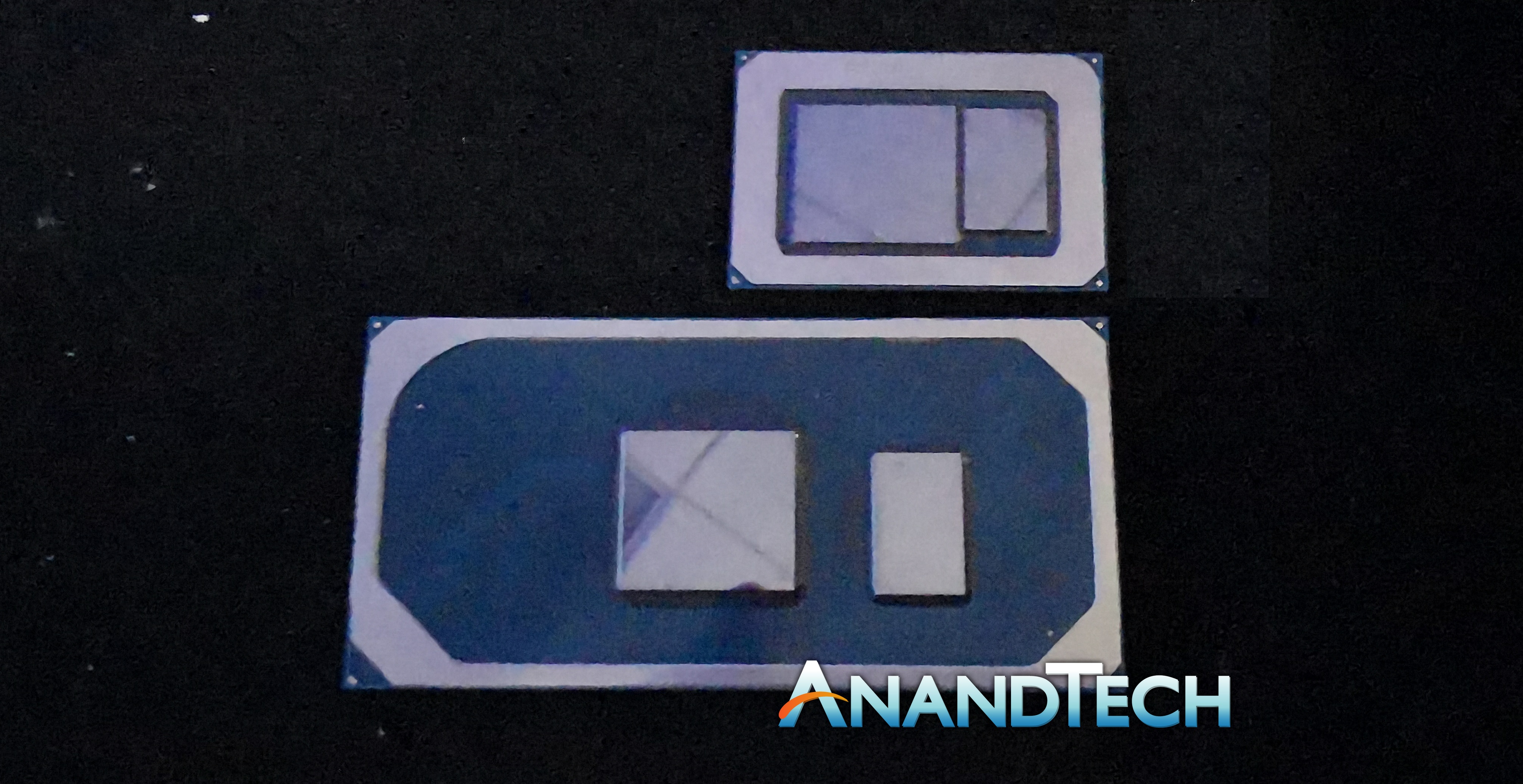
This Type-4 option also uses the ‘recessed in board’ design we first saw with Broadwell-Y, which is required based on the integrated voltage regulators that Intel now uses on its low powered designs. This makes a very interesting point about Intel’s capabilities with low powered 10nm designs: one could postulate that as the recessed model is well above the traditional Y-series power line. If the 10nm process doesn’t go low down enough in power to that sub-5W range, it could either be because of power, or there isn't enough frequency for Intel to actually sell at volume. Alternatively Intel could end up increasing the base power of the Y-series. One could draw parallels with the first generation 10nm Cannon Lake Core i3-8121U at 15W, which was initially postulated to be dual-core Y-series silicon, rather than the 15W U-series designation it ended up with (our review showed that it did indeed consume more power for the same work compared to a 14nm equivalent design, which would imply a very high static power). With this in mind, it makes me wonder what percentage of Type 3 / Type 4 package designs Intel will end up shipping into the market.
Broadwell Motherboard Design for Recessed Power Implementation
Intel is keen to promote that one of the new features of Ice Lake is its Thin Magnetic Inductor Array, which helps the FIVR achieve better power conversion efficiencies and waste less power. The main issue with a FIVR is at low power consumption states that have a lot of inefficiency – some other processor designs have a linear LDO (Low-Dropout Regulator) implementation which is better for low power designs but less efficient in high power modes.
Using Power More Efficiently: Dynamic Tuning 2.0
A common thread in modern microprocessor design is being able to use the power budget available. There have been many articles devoted to how to define power budgets, thermal budgets, and what the mysterious ‘TDP’ (thermal design power) actually means in relation to power consumption. Intel broadly uses TDP and power consumption simultaneously, along with a few other values, such as power limits 1 and 2 (PL1 and PL2), which apply to sustained power draw and peak power draw respectively. Most Intel processors up until this point will allow a processor to turbo, up to a peak power draw of PL2 for a fixed time, before enforcing a PL1 sustained power draw. This is all very OEM dependent as well. However, for Ice Lake, this changes a bit.
For Ice Lake, Intel has a new feature called Dynamic Tuning 2.0, which implements a layer of machine learning on top of the standard turbo mode. The idea behind DT2.0 is that the processor can predict the type of workload that is incoming, say transcode, and adjust the power budget intelligently to give a longer turbo experience.
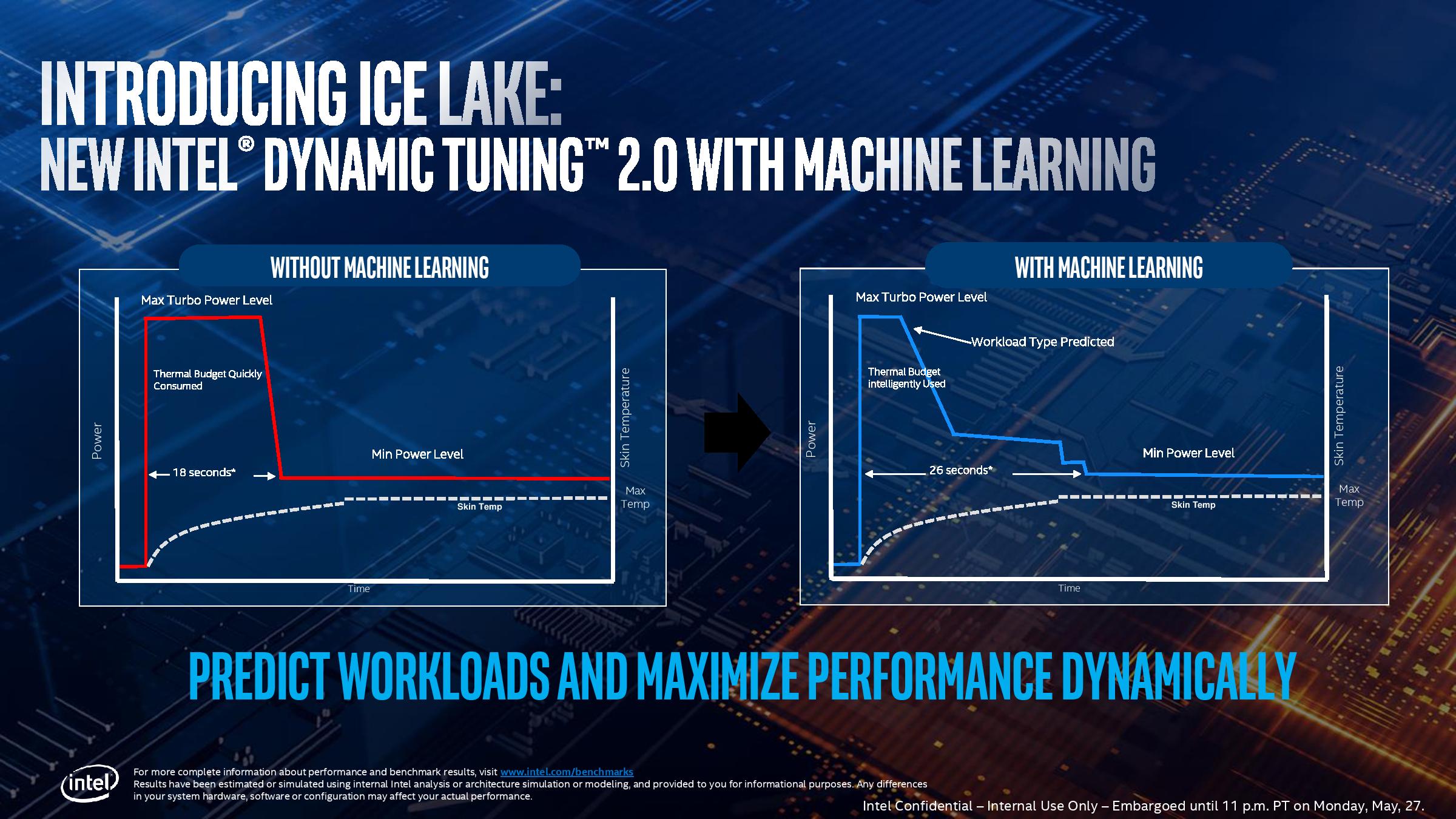
Technically the concepts of PL1 and PL2 don’t magically disappear under this new regime – the processor ends up going below max turbo because the algorithm predicts that the user won’t need it, and this saves up ‘power budget’ in order to enable the turbo to work for longer.
This is a topic that Intel will hopefully go into more detail. We do know that it requires collaboration at the OS level, but how these algorithms are trained would be a useful trove of information. It is unclear whether Intel will allow this feature to be enabled/disabled at the user level, for testing purposes, but it should be noted that unless it is by default ‘on’ for OEM systems, we might end up with some systems enabling it while others do not.
Thunderbolt 3: Now on the CPU*
One of the big failures of the Thunderbolt technology since its inception has been its adoption beyond that Apple ecosystem. In order to use it, both the host and the device needed TB controllers supplied by Intel. It wasn’t until Thunderbolt 3 started to use USB Type-C, and Thunderbolt 3 having enough bandwidth to support external graphics solutions, that we started to see the number of available devices start to pick up. The issue still remains that the host and device need an expensive Intel-only controller, but the ecosystem was starting to become more receptive to its uses.
With Ice Lake, that gets another step easier.
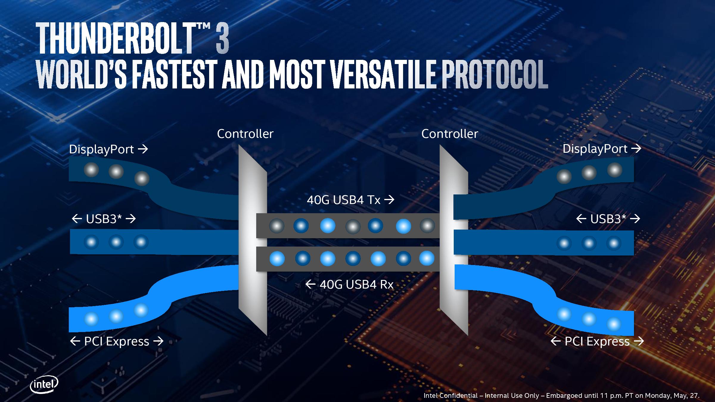
Rather than bundle TB3 support into the chipset, Intel has integrated it on the die of Ice Lake, and it takes up a sizable amount of space. Each Ice Lake CPU can support up to four TB3 ports, with each TB3 port getting a full PCIe 3.0 x4 root complex link internally for full bandwidth. (For those keeping count, it means Ice Lake technically has 32 PCIe 3.0 lanes total).
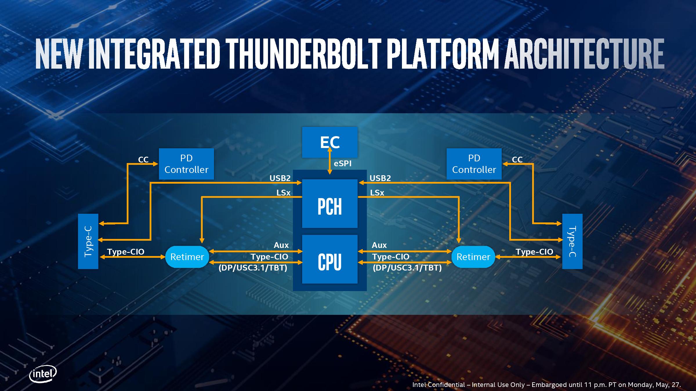
Intel has made it so each side of the CPU can support two TB3 links direct from the processor. There is still some communication back and forth with the chipset (PCH), as the Type-C ports need to have USB modes implemented. It’s worth noting that TB3 can’t be directly used out of the box, however.
Out of the four ports, it will be highly OEM dependent on how many of those will actually make it into the designs – it’s not as simple as just having the CPU in the system, but other chips (redrivers) are needed to support the USB Type-C connector. Power delivery too requires extra circuitry, which costs money. So while Intel advertises TB3 support on Ice Lake, it still needs something extra from the OEMs. Intel states that a retimer for the integrated solution is only half the size compared to the ones needed with the TB3 external chips, as well as supporting two TB3 ports per retimer, therefore halving the number of retimers needed.
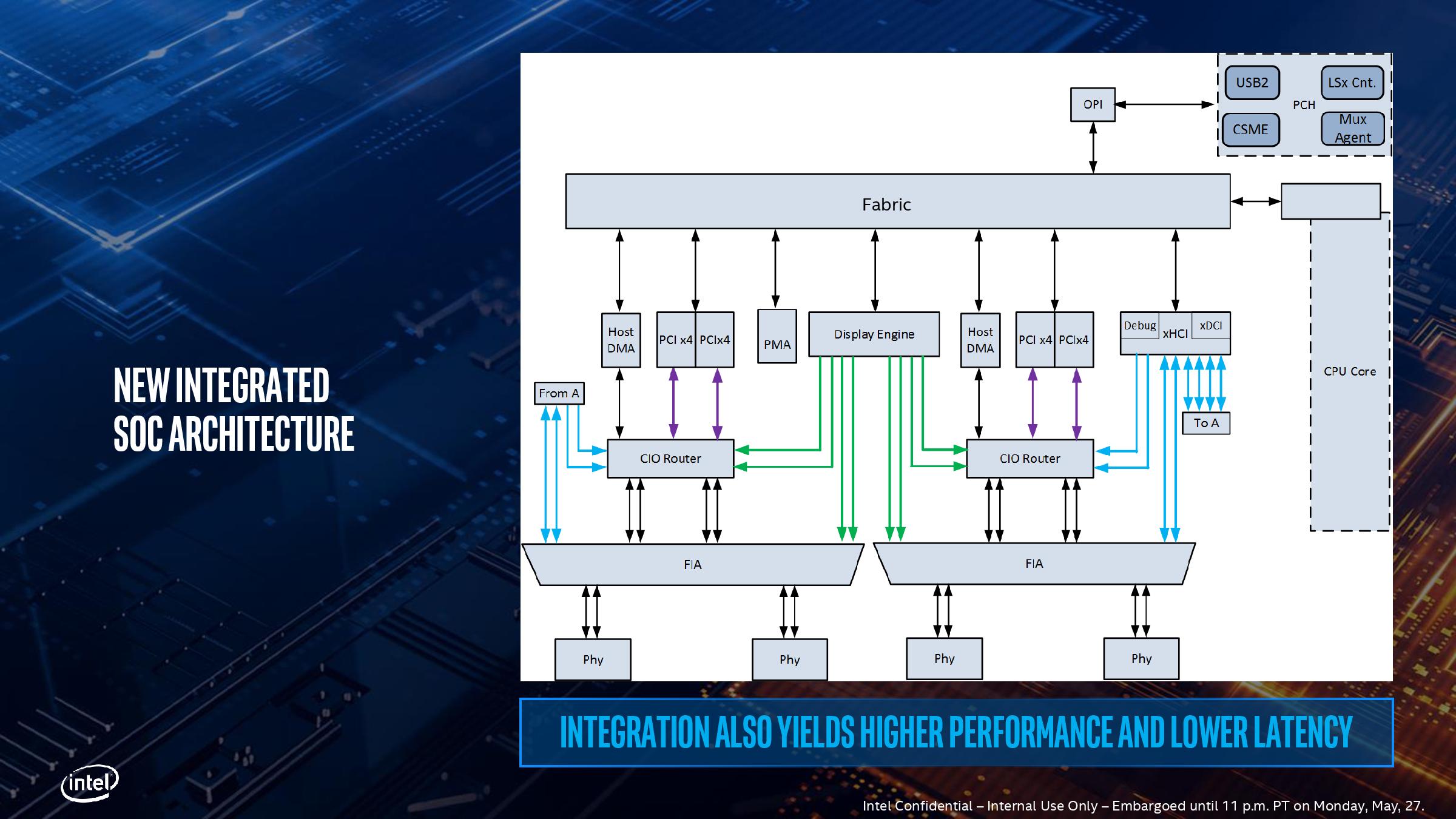
Here’s a more detailed schematic, showing the complexities of adding in TB3 into a chip, with the four PCIe x4 complexes shown moving out to each of the individual PHYs at the bottom, and connected back into the main SoC interconnect fabric. The display engine also has to control what mode the TB3 ports are in, and what signals are being sent. Wake up times for TB3 in this fashion, according to Intel, are actually slightly longer compared to a controller implementation, because the SoC is so tightly integrated. This sounds somewhat counterintuitive, given that the requisite hardware blocks are now closer together, but it all comes down to power domains – in a separate chip design, each segment has a separate domain with individual power up/down states. In an integrated SoC, Intel has unified the power domains to reduce complexity and die area, which means that more careful management is required but latency ultimately increases a little bit.
The other upside to the tightly coupled integration is that Intel stated that this method of TB3 is a lot more power efficient that current external chip implementations. However they wouldn’t comment on the exact power draw of the TB3 block on the chip as it corresponds to the full TDP of the design, especially in relation to localized thermal density (Intel was initially very confused by my question on this, ultimately saying that the power per bit was lower compared to the external chip, so overall system power was lower – they seemed more interested in discussing system power over chip power). Intel did state that the difference between an idle and a fully used link was 300 mW, which suggests that if all four links are in play, we’re looking at 1.2 W. When asked, Intel stated that there are three different power delivery domains within the TB3 block depending on the logic, that the system uses integrated voltage regulation, and the TB3 region has an internal power rail that is shared with some of the internal logic of the CPU. This has implications when it comes to time-to-wake and idle power, but Intel believes it has found a good balance.
Regarding USB4 support, Intel stated that it is in the design, and they are USB4 compliant at this point, but there might be changes and/or bugs which stop it from being completely certified further down the line. Intel said that it ultimately comes down to the device side of the specification, although they have put as much in as they were able given the time constraints of the design. They hope to be certified, but it’s not a guarantee yet.
Depending on who you speak to, this isn’t Intel’s first crack at putting TB3 into CPU silicon: the chip that Intel never wants to talk about, Cannon Lake, supposedly also had an early TB3 design built inside that never worked. But Intel is confident in its Ice Lake implementation, especially with supporting four ports. I wouldn’t be surprised if this comes to desktop when Intel releases its first generation 10nm desktop processors.
*The asterisk in the title of this page is because you still need external hardware in order to enable TB3.
Wi-Fi 6: Implementing AX over AC*
In consumer products, Intel has been placing its new Wi-Fi initiative into every chipset it can find. We’ve seen CNVi-enabled solutions occur on the desktop and in the notebook space for almost two years now, with the goal to make high-performance and low-power Wi-Fi ubiquitous, and to push Intel’s wireless solutions everywhere. Ice Lake is where Intel enables Wi-Fi 6 in such a solution.
If you’ve never come across the term CNVi before, it is Intel’s proprietary interface link and controller which connects the logic parts of the wireless connection on the chipset to the antenna and radio frequency analog parts which are found on a different module. This allows Intel’s partners to use different antenna ‘RF’ modules depending on what it wants to support, such as single antenna designs, dual antenna designs, or higher bandwidth modes.
Because CNVi is a proprietary interface, Intel has no plans to license it, and therefore the only RF modules you can buy to support it come from Intel. Intel states that its CNVi solution enables the high frequency digital logic to be built on its 14nm process with the chipset, and the RF analog side can be built on 28nm UMC which is better for analog signals and performance than any of Intel’s currently available manufacturing processes. Overall Intel states that using an external RF chip in this fashion affords a 15% silicon package reduction and a 40% pin reduction.

CNVi RF modules can either be an M.2 module (2230 = 22mm x 30mm) or as a soldered module (1216), which respectively allows for modularity, or for decreasing z-height for thin and light designs. Intel also states that this method of supplying the Wi-Fi, as separate digital and analog silicon, allows Wi-Fi certification to be done at the module level, rather than at the system level, simplifying the process for its partners.
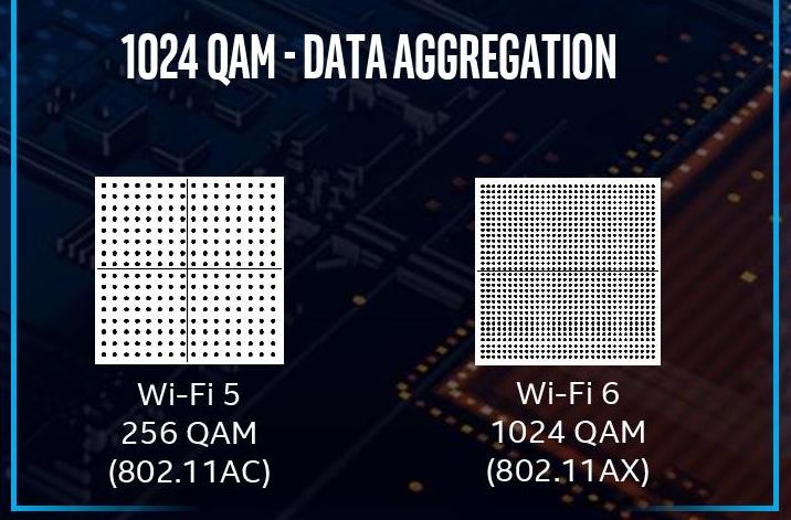
As an overarching technology, Wi-Fi 6 promises better bandwidth than standard Wi-Fi 5, as well as support for more devices on the same network. Technically this increased bandwidth comes down to data/time aggregation through the air as a benefit of OFDMA support, as well as 1024-QAM signaling design rather than 256-QAM signaling for increased throughput.

Wi-Fi 6 also has a lot of additional optional elements to the standard, which Intel believes will cause a good deal of confusion in the market. Naturally, Intel suggests that its partners that use a CNVi Wi-Fi 6 implementation also promote Wi-Fi 6 access points built on Intel’s platforms for simpler integration.
At this point in time, there are two main Wi-Fi 6 controllers: Intel’s AX200/AX201 2x2 CNVi module which uses the on-die enhancements, and Rivet Network’s AX1650 M.2 module which doesn’t use any of the on-die enhancements as it connects through a PCIe lane on the chipset. Technically both are built with the same silicon, as the companies are working together on the design, however Rivet is implementing its own acceleration techniques due to engines inside the hardware.
*The asterisk in the title of this page is because you still need external hardware in order to enable it, and to do it in the best way requires Intel-only hardware. You can use other vendor hardware, but you don’t need something special on the SoC to enable that.
Performance Claims:
+18% IPC vs. Skylake,
+47% Performance vs. Broadwell
With every new product generation, the company releasing the product has to put some level of expectations on performance. Depending on the company, you’ll either get a high level number summarizing performance, or you’ll get reams and reams of benchmark data. Intel did both, especially with a headline ‘+18%’ value, but in recent months the company has also been on a charge about what sort of benchmarking is worth doing. I want to take a quick diversion down that road, and give my thoughts on the matter.
First, I want to define some terms, just so we’re all on the same page.
- A synthetic test is a benchmark engineered to probe a feature of the processor, often to find its peak capability in one or several specific task. A synthetic test does not often reflect a real-world scenario, and likely doesn’t use real world software. Synthetic benchmarks are designed to be stable and repeatable, and the analysis often describing how a processor performs in an ideal scenario.
- A real-world test uses software that the user ends up using, along with a representative workload for that software. These tests are usually most applicable to end-users looking to purchase a product, as they can see actual use-case results. Real-world tests can have obvious pitfalls: it can be hard to test across multiple machines with only a single license, and testing one piece of software has no guarantee on performance on another.
A typical analysis of a processor does two things: what can it do (synthetic) and how does it perform (real-world). Users interested in the development of a platform, how it will expand and grow, or engineers peering over the fence, or even investors looking at the direction the company is going, will look at what products can do. People looking at what to use, what to work with, are more interested in the performance. Reviewers should get this concept, and companies like Intel should get this too – with Intel hiring a number of ex-reviewers of late, this is coming through.
A couple of months ago, Intel approached subsets of reviewers to discuss best benchmarking practices. On the table were real-world benchmarks, and which benchmarks represent the widest array of the market. Under fire was Cinebench, a semi-synthetic test (it uses a real-world engine on example data) that Intel believed didn’t represent the performance of a processor.
Intel provided data from one of its commissioned surveys on software that people use. Their data was based on a list of all consumers, from entry-level users up to prosumers, casual gamers, and enthusiasts, but also covering commercial use cases. At the top of the list were the obvious examples, such as OS and browsers: Explorer.exe, Edge, Chrome. In the top set were important widely distributed software packages, such as Photoshop (all versions), Steam, WinRAR, Office programs, and popular games like Overwatch. The point Intel was trying to make with this list is that a lot of reviewers run software that isn’t popular, and should aim to cover the widest market as possible.
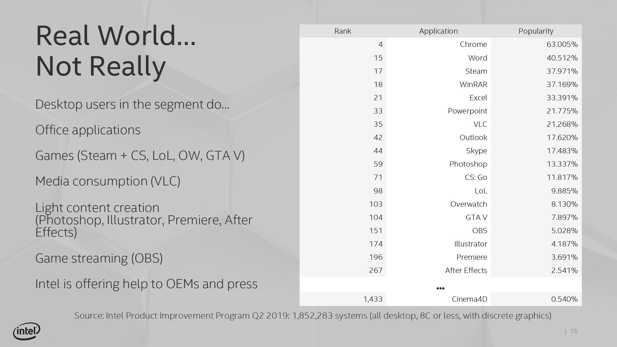
The key point they were trying to make was that Cinebench, while based on Cinema4D and a rendering tool used by a number of the community, wasn’t the be-all and end-all of performance. Now this is where Intel’s explanation became bifurcated: despite this being a discussion on what benchmarks reviewers should consider using, Intel’s perspective was that citing a single number, as Intel’s competitors have done, doesn’t represent true performance in all use cases. There was a general feeling that users were taking single numbers like this and jumping to conclusions. So despite the fact that the media in the room all test multiple software angles, Intel was clear in that they didn’t want a single number to dominate the headlines, especially when it’s from software that is ranked (according to Intel’s survey) somewhere in the 1400s.
Needless to say, Intel got a bit of backlash from the press in the room at the time. Key criticisms were that those present, when they get hardware, test a variety of software, not just Cinebench, to try and give a more overall view. Other key elements included that the survey covered all users, from consumer, commercial, and workstation: a number of the press in the room have audiences that are enthusiasts, so they will cater their benchmark accordingly. There was also a discussion that a number of software packages listed in the top 100 are actually difficult to benchmark, due to licensing arrangements designed to stop repeated installs across multiple systems. Typically most software vendors aren’t interested in working with the benchmark community to help evaluate performance, in the event that it exposes deficiencies in their code base. There was also the way in that readers were adapting over time: most focused readers want their specific software tested, and it is impossible to test 50 different software packages, so a few that can be streamlined in a benchmark suite are used as a representative sample, and typically Cinebench is one of those in the rendering arena, alongside POV-Ray, Corona, etc.
Intel, at this stage in the discussion, still went on to show how the new hardware performs on a variety of tests. We’ve covered these images before on previous pages, but Intel stated a significant uplift in graphics compared to the current 14nm offerings, from 40% up to 108%:
As well as comparisons to the competition:
Aside from 3DMark, these are all ‘real-world’ tests.
Move forward a few weeks, and Intel’s Tech Day where Ice Lake is discussed, and Intel brings up IPC.
Intel’s big statement is that Sunny Cove, a 2019 product, offers 18% more instructions per clock against Skylake, a 2015 product. In order to come to that conclusion, as expected, Intel has to turn to synthetic testing: SPEC2006, SPEC2017, SYSMark 2014 SE, WebXPRT, and Cinebench R15. Wait, what was that last one? Cinebench?
So there are two topics to discuss here.
First is the 18% increase over four years – that’s the equivalent to a 4.2% compound annual growth rate. Some users will state that we should have had more, and that Intel’s issues with its 10nm manufacturing process means that this should have been a 2017 product (which would have been an 8.6% CAGR). Ultimately Intel built enough of an IPC increase lead over the last decade to afford something like this, and it shows that there isn’t an IPC wall just yet.
Second is the use of Cinebench, and the previous version at that. Given what was discussed above, various conclusions could be drawn. I’ll leave those up to you. Personally, I wouldn’t have included it.
Aside from IPC, Intel also spoke about actual single-threaded performance about Sunny Cove in its 15W mode.

At a brief glance, I would have expected this graph to be from real-world analysis. But given the blurb at the bottom it shows that these results are derived from SPEC2006, specifically 1-thread int_rate_base, which means that these are synthetic results, so we’ll analyze them with that in mind. This test also gets lots of benefit from turbo, with each test likely to fit inside the turbo window of an adequately cooled system.
The base line here is Broadwell, Intel’s 5th Generation processor, which if you remember was the first Intel processor to have an integrated FIVR on the mobile parts for power efficiency. In this case we see that Intel puts Skylake as +9% above Broadwell, then moving through Kaby Lake and Whiskey Lake we see the effect of increasing that peak turbo frequency and power budget: when we moved from dual core to quad core 15W mobile processors, that peak turbo power budget increased from 19W to 44W, allowing longer turbo. Overall we hit +42% for 8th Gen Whiskey Lake over Broadwell.
Ice Lake, by comparison, is +47% over Broadwell. When moving from Broadwell to Ice Lake, which Intel expects most of its users to do, that’s a sizable single threaded performance jump, I won’t dispute that, although I will wait until we see real world data to come to a better conclusion.
However, if we compare Ice Lake to Whiskey Lake, we see only a +3.5% increase in single threaded performance. For a generation-on-generation increase, that’s even lower than the four-year CAGR from Skylake. Some of you might be questioning why this is happening, and it all comes down to frequency.
Intel’s current 8th Gen Whiskey Lake, the i7-8565U, has a peak turbo frequency of 4.8 GHz. In 15W mode, we understand that the peak frequency of Ice Lake is under 4.0 GHz, essentially handing Whiskey Lake a ~20% frequency advantage.
If this sounds odd, turn over to the next page. Intel is going to start tripping over itself with its new product lines, and we’ll do the math.
Competing Against Itself: 3.9 GHz Ice Lake-U on 10nm vs 4.9 GHz Comet Lake-U on 14nm
At the same time that Intel is releasing Ice Lake, we have confirmed from multiple sources that the company intends to release another generation of mobile products based on 14nm as well. This line of hardware, also called Intel 10th Gen Core, will be under the internal codename ‘Comet Lake’, and go after a similar power distribution to what Ice Lake will. There are a few differences in the design worth noting, and a big one that Intel will have a hard time organizing its marketing materials for.
The differences between Ice Lake-U and Comet Lake-U are set to be quite confusing. Leaks from various OEMs about upcoming products give us the following:
Ice Lake: The Core i7-1065G7
Ice Lake-U hardware, based on 10nm, will be given a ‘G’ in the product name, such as i7-1065G7. This breaks down such that
- i7 = Core i7
- 1065 = from the 10th Gen Core
- 1065 = position ‘65’ relative to the rest of the other Ice lake processors,
- G7 = ‘Graphics Level 7’, which we believe to be the highest.
Intel has stated that the Ice Lake-U hardware will come in at 9W, 15W, and 28W, as described in the previous pages, offering a highest turbo clock of 4.1 GHz, 64 EUs of Gen11 graphics, suitable for up to 1.1 TF of FP64 calculations. We suspect that the 4.1 GHz turbo frequency will be given to the 28W model following previous Intel launches, which means that the 15W part is likely to turbo to a few hundred MHz lower. Based on the Ice Lake plans we know, it seems that Intel is only targeting up to quad-core designs, but Ice Lake does support LPDDR4. Due to using the 10nm process, and with additional power refinements, Ice Lake hardware is expected to have longer a battery life compared to Comet Lake, although we will see this in product reviews through the year.
Comet Lake: The Core i7-10510U
Contrast this to Comet Lake-U, which is another round of processors based on 14nm. OEMs have given some light onto these processors, which should offer up to six cores. The naming of the processors follows on from the 8th Gen and 9th Gen parts, but is now under 10th Gen. This means that the Core i7-10510U breaks down as:
- i7 = Core i7
- 10510 = from the 10th Gen Core family,
- 10510 = position ‘51’ relative to the rest of Comet Lake
- U = U-series processor, 15-28W
OEM listings have shown Comet Lake-U to turbo up to 4.9 GHz on the best quad-core processor, while we have seen 9th gen hardware hit 5.0 GHz in the larger H-series designs.
For a full side-by-side comparison:
| Ice Lake-U vs Comet Lake-U | |||||
| Ice Lake-U* | AnandTech | Comet Lake-U* | |||
| 10+ | Lithography | '14nm class' | |||
| i7-1065G7 | Example CPU Name | i7-10510U | |||
| 9W 15W 28W |
TDP Options | 15W 28W? Same as 9th Gen? |
|||
| Up to 4C | Core Counts | Up to 6C (expected) | |||
| Sunny Cove | CPU Core | Skylake+++ | |||
| Up to 64 EUs Gen11 |
GPU GT2 Core | Up to 24 EUs Gen9.5 |
|||
| 3.9G (15W) 4.1G (28W) |
Highest Turbo | 4.9G? (15W) 5.0G+ ? |
|||
| DDR4-3200 LPDDR4-3733 |
DDR | DDR4-2667 LPDDR3-2133 |
|||
| AVX-512 | AVX | AVX2 | |||
| *All details are not yet confirmed by Intel, but shown on partner websites/trusted sources | |||||
Should Intel go ahead with the naming scheme, it is going to offer a cluster of mixed messages, even to end-users that understand the naming scheme. For those that don’t, there might not be an obvious way to tell a 10th Gen Ice Lake system and a 10th Gen Comet Lake system part from just reading the specification sheet, especially if the vendor lists it just as ‘10th Gen Core i7’.
Intel is trying to mitigate some of this with Project Athena, which is a specification for premium 10th Gen designs. In order to meet Athena specifications, you technically don’t need to have an Ice Lake processor, but it definitely does help with the graphics and battery life targets. We’re unsure at this point if Intel will add in distinct labeling to Athena approved devices or not, but this might be one way to discern between the two. The other is to look for the letter: G means Ice Lake, U means Comet Lake.
So the question is about what matters most to users?
If you want raw CPU frequency and cores, then Comet Lake still has benefits there, even if we add on Intel’s expected ‘+18%’ IPC claims. It would all come down to how the turbo plays out in each device, and Intel states that it is working closer than ever before with its OEM partners to optimize for performance.
Ice Lake systems on the other hand are going to offer better graphics, are initially all likely to be under the Project Athena heading, and provide good connectivity (Wi-Fi 6), good displays, and really nice battery life for the class of device. Ice Lake is going to play more in the premium space too, at least initially, which might indicate that Comet Lake could be angled down the price bracket.
To be honest, we should have been expecting this. When Dr. Murthy Renduchintala joined Intel a couple of years ago, he was quoted as saying that he wants to disaggregate the ‘generation’ from the lithography, and offer a range of products within each generation. The fruits of that campaign started with the last round of mobile platforms, and the fruits of that endeavor will ripen through the Ice Lake/Comet Lake kerfuffle*. It’s going to be agonizing to tell users the difference, and even more so if OEMs do not list exact CPU specifications in their online listings. Intel has been so forthright with two distinct brands, the ‘X’ Gen Core and the Core ‘i7/i5/i3’ naming, that now both are ultimately meaningless to differentiate between two different types of products.
What should be the solution here? On initial thoughts, I would have pushed Ice Lake as an 11th Gen Core. It’s a new and exciting product, with a updated microarchitecture, better graphics, and leading edge lithography, along with Project Athena, it needs to be categorically separated from any other processors it might be competing with. It’s either that, or come up with an alternative naming scheme for it all. At this point, Intel is heading to a sticky mess, where it’s competing against itself and the casual user who hasn’t done meticulous research might not end up with the optimum product.
*To be clear, in the past, Intel used to separate product line microarchitecture based on the nth Gen Core designation. This does not happen anymore – a single ‘nth Gen Core’ brand might have 3+ different microarchitectures depending on what product you are looking at. It is ultimately confusing for any end-customers that have a passing knowledge of Intel’s product lines, and highly annoying to anyone with technical prowess discussing Intel’s products. I hate it. I understand it, but I hate it.
Intel’s Ice Lake and Sunny Cove
A Welcome Update, with Questions on Execution
When launching a new mobile product using a new processor design, all the parts have to come together to make it work. This means all of the following:
- The microarchitecture design
- SoC implementation
- Manufacturing
- Co-operation with partners/OEMs
- Time to Market
- Messaging
- Marketing
- Interactions with the press and consumers
- Promotion
- Price
- Competitiveness
Any one of these segments could make or break the next wave of innovation (a key phrase Intel likes to use). With Intel’s 10nm manufacturing process, and the 10th Gen Core 'Ice Lake' design, we’re moving along each of these points in turn, and it is interesting to see what the final reflection will be several years down the line. From our perspective, we now have extensive details on the core and the SoC, and Intel is slowly moving into product phase by the end of the year. We can evaluate what we’ve seen.
The Core and the SoC
Having ‘not another Skylake’ is a huge sigh of relief. With every new microarchitecture update, especially significant ones, we like to see how the power budget is being used and what key structures within the microarchitecture have been improved and expanded upon. The team behind the Sunny Cove core have listed some impressive hard numbers, with doubling the L1 store bandwidth, making significant L1 and L2 cache adjustments, increasing the reorder buffer a whopping +57%, and moving to a 10-port execution unit design. The inclusion of AVX-512 is welcomed by parts of the community for sure, although I expect not as many as Intel would like (this leads onto Intel’s DLBoost strategy, I’ll mention later). Assuming we can get the same +18% IPC metrics that Intel does, this is a great uplift and it will be exciting to see where we go from here.
On the SoC, the big improvements to the graphics and the memory controller are my important ones here. Intel is taking integrated graphics seriously again, with an improved 64 EU design that promises to match AMD’s best at 25W. Intel has improved its memory controller significantly here, now supporting LPDDR4-3733 and DDR4-3200, which helps given that the graphics hardware is always craving memory bandwidth.
Adding Thunderbolt 3 to the SoC is going to help drive adoption in the mobile space, however speaking to a number of press, we think that because TB3 still requires an expensive controller on the device end, that the standard still has that high-cost to entry barrier, even if it ends up being cheaper for host implementation. Until non-Intel TB3 device controllers hit the market, the biggest benefit here is going to be potential support for the USB4 standard. With respect to the Wi-Fi 6 enablement, I’m not so enthused here, as it still requires an additional Intel-only proprietary CNVi module, forcing OEMs to go down an Intel route. If Intel made the CNVi standard open to all, I’d be making a bigger deal about this.
Manufacturing and Time To Market
The fact that Intel is going to end up competing against itself, with Ice Lake-U against Comet Lake-U, is akin to shooting yourself in the foot. Ultimately we expect Ice Lake-U to be focused on the premium market through Intel’s Project Athena, but Comet Lake-U is likely to span from budget to premium as well, especially if it ends up supporting more cores than Ice Lake. Ice Lake should have been a 2017 product, and Intel is only now at a point where it believes its 10nm products are viable for the market, which leads to questions on if the process is even profitable, and how many chips are going to be made available to OEMs – again, because of Project Athena, only key OEM customers going for those premium devices are going to launch initially, tailoring the messaging towards that premium feel.
Questions still surround Intel’s 10nm viability, especially given that the company has promised it is going to be producing high core count Xeons on this process node. Hopefully we can get an update on that.
Ice Lake Messaging, and Project Athena
As mentioned, the whole deal with Whiskey Lake and Comet Lake single thread CPU performance being similar to Ice Lake is going to be a mess. Part of this is down to the messaging for sure, whereby both Ice Lake and Comet Lake are going to be Intel 10th Gen, with Core i7 and Core i5/i3 variants. The only way to distinguish between the two is that Ice Lake has a G in the SKU and Comet Lake has a U, details that some of Intel’s own partners don’t disclose on product pages on websites.
One thing that Intel could lean on is the AVX-512 in Ice Lake, and its DL Boost strategy. Despite AVX-512 being inside Intel’s Xeons, the amount of ‘consumer-grade’ software that uses it is very minimal. By moving it into the consumer platforms, and enabling features like VNNI, Intel wants to drive AI-software solutions into the market. One example we were given was the ability for image software to sort images by what it detects in them – and having this all done locally (and securely) on the CPU, rather than the cloud. If Intel can execute on DL Boost for consumers, it could be a big win, and an easy benefit over the competition.
Turning to Project Athena – I’m all in favor of driving innovation forward and defining specifications that help push new and innovative form factors to enhance the user experience. But as you might have guessed, as it stands, I’m not its biggest fan. The Athena ecosystem is its own closed playground – in order for OEMs to play ball, they have to meet a number of requirements, a sizable chunk of which are only beneficial through Intel-only hardware. For example, Athena devices need Wi-Fi 6, which can be provided by an M.2 module or a CNVi RF chip. Athena devices also need substantial battery life, and the best way to achieve that is by using a CNVi RF option – but Intel is the only one that can make them because the CNVi standard is proprietary.
If an OEM doesn’t want to use Intel’s Wi-Fi 6 solution, then it makes it harder to develop an Athena certified device. It means that OEMs have to play Intel’s game in order to compete in the space. For me, that’s a high entry fee. Sure, the certified devices at the end of day are likely to be great, but if they all have Intel Wi-Fi 6, then where’s the variation? Perhaps I’m a little altruistic here: Intel is trying to create its own certification program and to play by the rules might require investing in Intel-only designed controllers. But I feel that an effort like this works best when there’s competition at every level.
Competition
On a core-to-core level, Intel's recent designs have the following configurations:
| Microarchitecture Comparison | ||||||
| Skylake | Cannon Lake | Sunny Cove* | Zen | Zen 2 | ||
| L1-D Cache |
32 KiB/core 8-way |
32 KiB/core 8-way |
48 KiB/core 12-way |
32 KiB/core 8-way |
32 KiB/core 8-way |
|
| L1-I Cache |
32 KiB/core 8-way |
32 KiB/core 8-way |
32 KiB/core 8-way |
64 KiB/core 4-way |
32 KiB/core 8-way |
|
| L2 Cache |
256 KiB/core 4-way |
256 KiB/core 4-way |
512 KiB/core 8-way |
512 KiB/core 8-way |
512 KiB/core 8-way |
|
| L3 Cache |
2 MiB/core 16-way |
2 MiB/core 16-way |
2 MiB/core 16-way |
2 MiB/core | 4 MiB/core | |
| L3 Cache Type | Inclusive | Inclusive | Inclusive | Non-Inclusive | Non-Inclusive | |
| Decode | 4 + 1 | 4 + 1 | 4 + 1 | 4 | 4 | |
| uOP Cache | 1.5k | 1.5k | 2.25k | 2k | 4k | |
| Reorder Buffer | 224 | 224 | 352 | 192 | 224 | |
| Execution Ports | 8 | 8 | 10 | 10 | 11 | |
| AGUs | 2 + 1 | 2 + 1 | 2 + 2 | 1 + 1 | 2 + 1 | |
| AVX-512 | - | 1 x FMA | 1 x FMA | - | ||
| * Sunny Cove numbers for Client. Server will have different L2/L3 cache and FMA, like Skylake | ||||||
Where AMD has reduced the size of the L1-D cache (to fit in a 4k micro-op cache), Intel has increased it. Both AMD and Intel now sit with 512 KiB L2 caches, although AMD is 4 MiB of non-inclusive cache to Intel's 2 MiB of inclusive cache. Intel has a much larger re-order buffer, and made improvements to its address generation units to help feed the cores. It's becoming ever more important to feed the beast.
Final Thought of the Day
Looking through the Ice Lake and Sunny Cove design, I have to give kudos to Intel’s engineers. The core microarchitecture looks solid, and there is no doubt that Intel will have a raw single thread performance advantage in the mobile space. I’m glad that Intel is taking its graphics solutions seriously again, and between the CPU and GPU, it’s good to see that extra power budget going to good use. I can’t wait to have the hardware on hand.
If you’re listening Intel, please consider the following: I haven’t seen any plans to bring Ice Lake to the desktop, but can we get a quad-core Ice Lake-U at 35W in a desktop processor form factor, for $179?


