Original Link: https://www.anandtech.com/show/15973/the-intel-xelp-gpu-architecture-deep-dive-building-up-from-the-bottom
The Intel Xe-LP GPU Architecture Deep Dive: Building Up The Next Generation
by Ryan Smith on August 13, 2020 9:00 AM EST- Posted in
- Intel
- GPUs
- Tiger Lake
- Xe
- Xe-LP
- DG1
- Intel Arch Day 2020
- SG1
As part of today’s Intel Architecture Day, Intel is devoting a good bit of its time to talking about the company’s GPU architecture plans. Though not a shy spot for Intel, per-se, the company is still best known for its CPU cores, and the amount of marketing attention they’ve put into the graphics side of their business has always been a bit weaker as a result. But, like so many other things at Intel, times are changing – not only is Intel devoting ever more die real estate to GPUs, but over the next two years they are transitioning into a true third player in the PC GPU space, launching their first new discrete GPU in several generations.
As part of Intel’s previously-announced Xe GPU architecture, the company intends to become a top-to-bottom GPU provider. This means offering discrete and integrated GPUs for everything from datacenters and HPC clusters to high-end gaming machines and laptops. This is a massive expansion for a company whom for the last decade has only been offering integrated GPUs, and one that has required a lot of engineering to get here. But, at long last, after a couple of years of talking up Xe and laying out their vision, Xe is about to become a reality for Intel’s customers.
While we’ll focus on different Xe-related announcements in separate articles – with this one focusing on Xe-LP – let’s quickly recap the state of Intel’s Xe plans, what’s new as of today, and where Xe-LP fits into the bigger picture.
When first announced back in 2018, Intel laid out plans for a single GPU architecture, Xe, comprised of three different microarchitectures: Xe-LP, Xe-HP, and Xe-HPC. Spanning the market from the bottom to the top respectively, Xe-LP would go into integrated and entry-level discrete graphics, Xe-HP into enthusiast and datacenter parts, and finally Xe-HPC would be for high performance computing clusters such as the upcoming Aurora supercomputer, the US Department of Energy’s long-awaited exaflop machine.
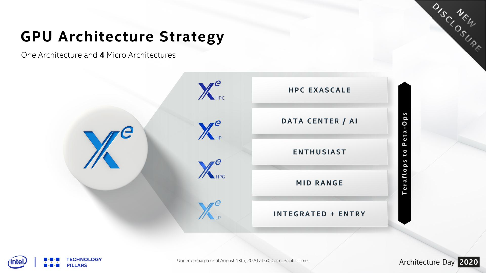
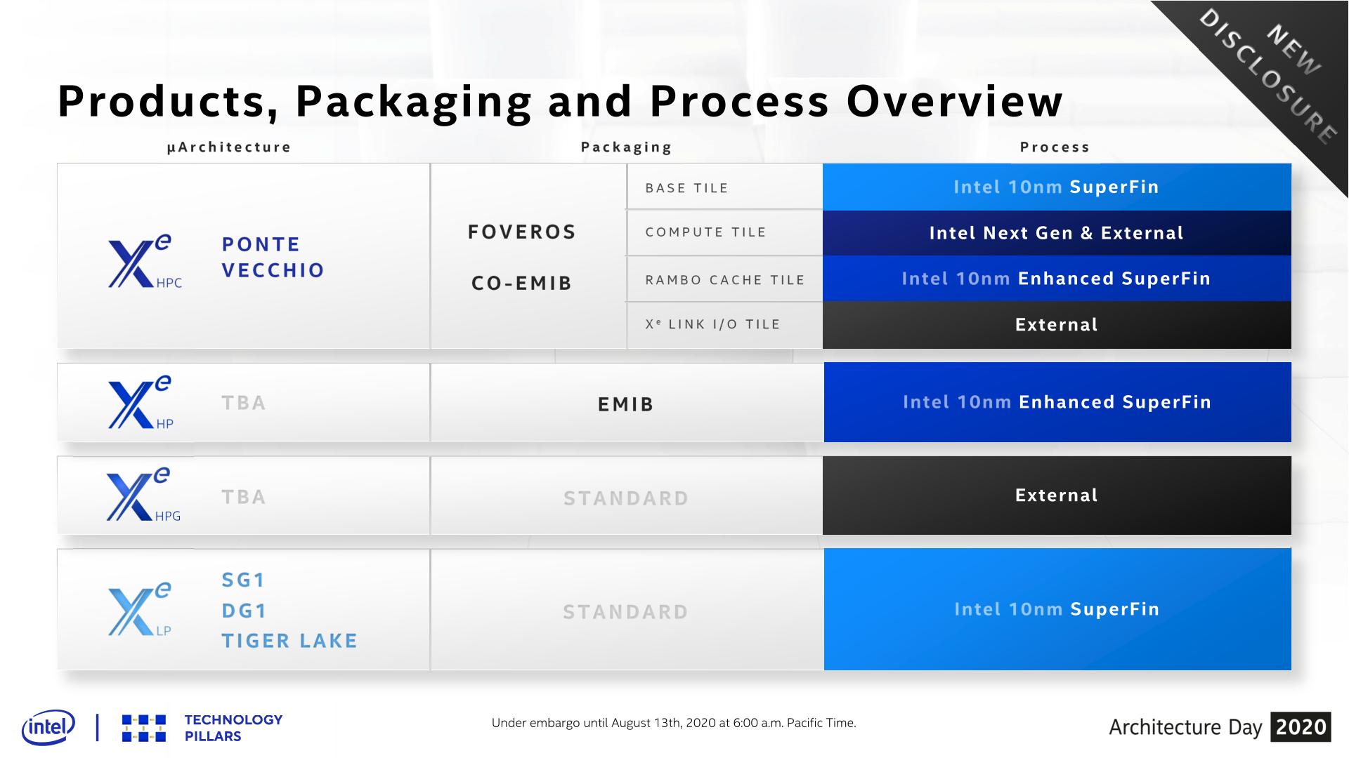
Since then, Intel has revised that plan a bit, and what was three microarchitectures is now four. Being announced as part of Intel Architecture Day today, Intel is revealing Xe-HPG, an additional microarchitecture for gaming-focused chips. We have more on Xe-HPG in this article, but at a high level it’s meant to be the missing piece of the puzzle in Intel’s product stack, offering a high-performance gaming and graphics-focused chip as opposed to Xe-HP, which is specializing in datacenter features like FP64 and multi-tile scalability. Xe-HPG is set to arrive in 2021, and notably will be built entirely at a third-party fab, unlike the rest of the Xe family.
Which to bring things back to the immediate topic of Xe-LP, makes this year’s launch of Intel’s first Xe microarchitecture all the more important. Intel’s plans for Xe involve building up successive Xe parts – quite literally in Xe-HPC’s case – going for wider designs that incorporate ever increasing numbers of base building blocks, and then scaling out the number of GPUs when even that isn’t enough. So Xe-LP is very much the foundation of the Xe family, not just in diagrams but in architecture as well; and consequently, what Intel has designed for Xe-LP will have repercussions for the entire Xe product stack.
Xe-LP: Integrated with Tiger Lake, But Discrete as Well
While Intel’s product plans for Xe have them eventually reaching far and wide, it’s only fitting that things start at the same place they always have for Intel’s GPUs: integrated graphics. Xe and Xe-LP will be making their first appearance in the market as part of Intel’s new Tiger Lake SoC, which the company will be launching on September 2nd. And despite the fact that Intel isn’t talking much about the product side of Tiger Lake itself – preferring to keep today about architecture and making September about products – Tiger Lake was very clearly the focal point for Xe-LP’s design. So Tiger Lake is the catalyst for it all, as we’ll see when discussing Xe-LP’s features.
Given Intel’s official disclosures today (never mind the many, many leaks), it’s clear that Tiger Lake parts are going to top out with a single Xe-LP slice. Which, new with this generation, is now 96 of Intel’s more fundamental GPU Execution Units (EUs). Overall, the company is targeting a 2x increase in performance over Ice Lake (Gen11) graphics,
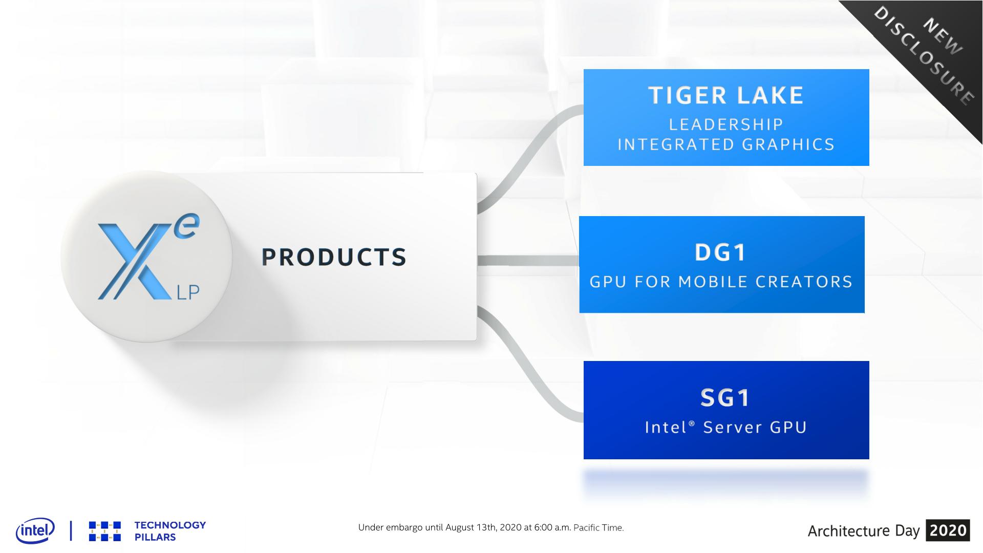
But Tiger Lake won’t be the only place where Xe-LP will show up. As previously disclosed by Intel, the company is developing a discrete GPU version of it, which they are calling DG1. Designed to be paired with Tiger Lake in notebooks and other mobile devices, DG1 is Intel’s first discrete GPU in over twenty years, and it’s the spiritual-successor of sorts to Intel’s GT3 and GT4e integrated GPU configurations. Only instead of building low-volume CPU designs with a larger GPU, Intel will instead sell OEMs a discrete GPU based on the same architecture and built on the same 10nm SuperFin process as the integrated GPU.
DG1 will be shipping this year, so expect to see it show up in higher-performing Tiger Lake laptops. However Intel is otherwise disclosing very little about the part, as they are not disclosing much of anything with regards to product configurations today. So while we know that it’s based on Xe-LP and that it’s mobile-focused (Intel has dropped all discussion of desktop usage), we don’t have official details on anything such as its configuration or what type of memory it uses.
And forming the final pillar, the sever space won’t be left out on Xe-LP either. Intel will be delivering a quad-GPU product for servers that they are calling SG1. Based on four DG1 GPUs, this will be a replacement of sorts for Intel’s Xeon Visual Compute Accelerator family of products. Designed to leverage Intel’s earlier integrated GPUs, the Xeon VCA cards were aimed at the video encoding market, using Intel’s QuickSync media blocks to accelerate the process. Now that Intel has discrete GPUs, they no longer need to gang together CPUs for this market, and instead can sell accelerators with just the GPU. It’s a bit of a niche market with regards to the larger GPU ecosystem, but it’s an important one for Intel, so they’re hoping that SG1 will make server operators stand up and take notice – or at least those pesky Goa'ulds.
Xe-LP Feature Set: DirectX FL 12_1 with Variable Rate Shading
Kicking off the proper part of our architectural deep dive, let’s start with a quick summary of Xe-LP’s graphics feature set. I call this a quick summary as there is unfortunately not a whole lot new to talk about here.
From an API-level perspective, Xe-LP’s feature set is going to be virtually identical to that of Intel’s Gen11 graphics. Not unlike AMD with their RDNA1 architecture, Intel has decided to concentrate their efforts on updating the low-level aspects of their GPU architecture, making numerous changes downstairs. As a result, relatively little has changed upstairs with regards to graphics features.
The net result is that Xe-LP is a DirectX feature level 12_1 accelerator, with a couple of added features. In particular, tier 1 variable rate shading, which was first introduced for Intel in their Gen11 hardware, is back again in Xe-LP. Though not as capable as the newer tier 2 implementation, it allows for basic VRS support, with games able to set it on a per-draw call basis. Notably, Intel remains the only vendor to support tier 1; AMD and NVIDIA have (or are) going straight to tier 2.
| DirectX 12 Feature Levels | ||||
| 12_2 (DX12 Ult.) |
12_1 | |||
| GPU Architectures | Intel: Xe-HPG? NVIDIA: Turing AMD: RDNA2 |
Intel: Gen9, Gen11, Xe-LP NVIDIA: Maxwell 2, Pascal AMD: Vega, RDNA (1) |
||
| Ray Tracing (DXR 1.1) |
Yes | No | ||
| Variable Rate Shading (Tier 2) |
Yes | No (Gen 11/Xe-LP: Tier 1) |
||
| Mesh Shaders | Yes | No | ||
| Sampler Feedback | Yes | No | ||
| Conservative Rasterization | Yes | Yes | ||
| Raster Order Views | Yes | Yes | ||
| Tiled Resources (Tier 2) |
Yes | Yes | ||
| Bindless Resources (Tier 2) |
Yes | Yes | ||
| Typed UAV Load | Yes | Yes | ||
The good news for Intel, at least, is that they were already somewhat ahead of the game with Gen11, shipping 12_1 support for even their slowest integrated GPUs before AMD had phased it into all of their products. So at this point, Intel is still at parity with other integrated graphics solutions, if not slightly ahead.
The downside is that it also means that Intel is the only hardware vendor launching a new GPU/architecture in 2020 without support for the next generation of features, which Microsoft & co are codifying as DirectX 12 Ultimate. The consumer-facing trade name for feature level 12_2, DirectX Ultimate incorporates support for variable rate shading tier 2, along with ray tracing, mesh shaders, and sampler feedback. And to be fair to Intel, expecting ray tracing in an integrated part in 2020 was always a bit too much of an ask. But some additional progress would always be nice to see. Plus it puts DG1 in a bit of an odd spot, since it’s a discrete GPU without 12_2 functionality.
Xe-LP By the Slice: 50% Larger With 96 EUs
Instead of focusing on high-level graphics features, the bulk of Intel’s attention has instead gone to the low-level architectural details of their GPUs. Xe-LP is the building block to many more Xe GPUs to come, so this is an area where Intel needed to get things right – both in design and power efficiency – in order to have a stable foundation for building future products.
And to be sure, that foundational analogy extents within Intel’s earlier GPU designs as well. While Xe is new branding and the start of something much bigger for Intel, it isn’t a clean sheet design of Intel’s GPUs. Rather it’s a focused evolution of Gen11, updating and replacing those bits that need to be altered for scalability or efficiency reasons. Consequently, there’s a good deal that is held over from Gen11, and the basic organizational structure of Intel’s GPUs remains the same.
| Intel GPU Specification Comparison | ||||||
| Xe-LP (Tiger Lake) |
Xe-HPG | Gen11 (Ice Lake) |
Gen9.5 (Kaby Lake) |
|||
| ALUs | 768 | Many | 512 | 192 | ||
| Texture Units | 48 | Lots | 32 | 12 | ||
| ROPs | 24 | Yes Please | 16 | 8 | ||
| Peak Clock | 1600MHz+ | Better Than Xe-LP | 1100MHz | 1150MHz | ||
| Throughput (FP32) | 2.46 TFLOPs | All of the FLOPs | 1.13 TFLOPs | 0.44 TFLOPs | ||
| Memory Clock | LPDDR4X-4266 | GDDR6 | LPDDR4X-3733 | DDR4-2133 | ||
| Memory Bus Width | 128-bit (IMC) |
Sizable | 128-bit (IMC) |
128-bit (IMC) |
||
| Geometry Rate (Prim/Clock) |
2 | 2x # of Slices | 1 | 1 | ||
| Manufacturing Process | Intel 10nm SuperFin | "External" | Intel 10nm | Intel 14nm+ | ||
| Architecture | Xe-LP | Xe-HPG | Gen11 | Gen9.5 | ||
| GPU | Tiger Lake Integrated |
Xe-HPG | Ice Lake Integrated | Kaby Lake Integrated | ||
| Launch Date | 09/2020 | 2021 | 09/2019 | 01//2017 | ||
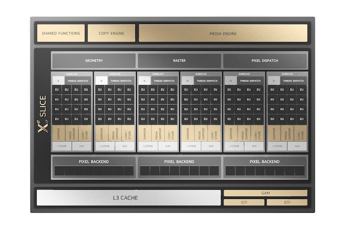
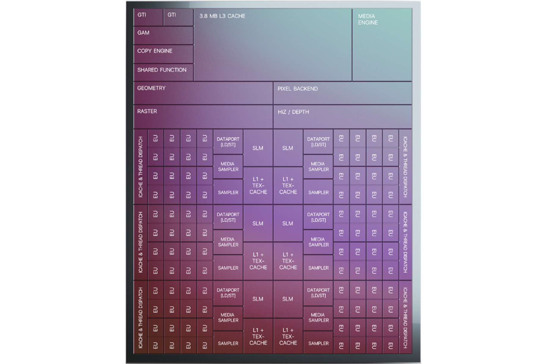
As always then, this means we’ll start with the Xe-LP Slice and Intel’s overall GPU design goals. Intel’s largest common building block, the company’s GPUs are organized into one or more slices, with a single slice containing a full copy of the core functional blocks needed for compute and rendering. This includes the geometry and raster frontend, thread dispatch hardware, the EUs themselves, texture units, and the ROP pixel backends.
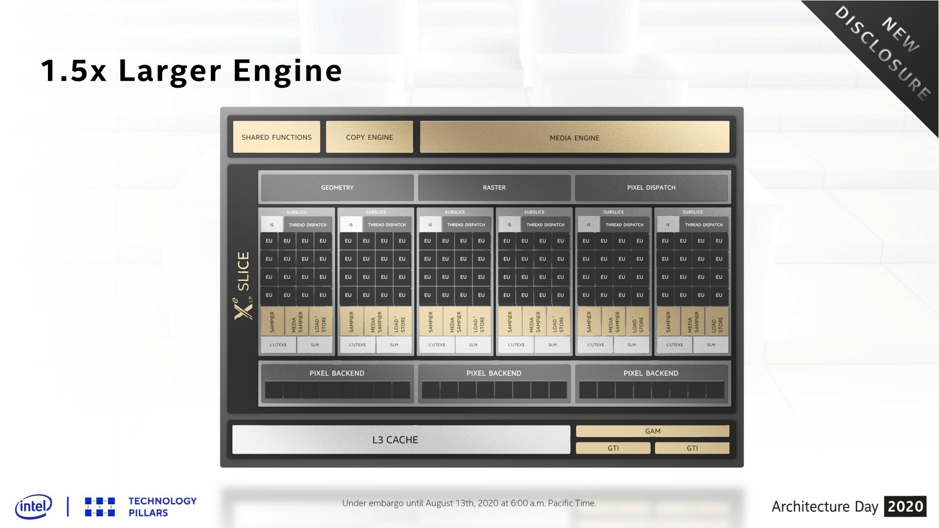
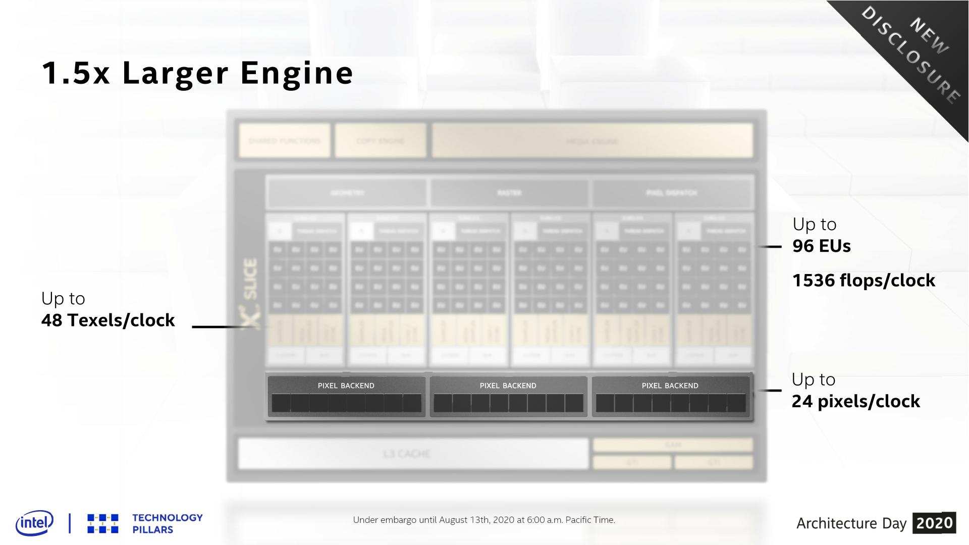
With Xe-LP, Intel has expanded almost everything about a slice by 50%. Which means that versus Intel’s Gen11 iGPUs, which happened to top out a single slice, there’s 50% more execution hardware to play with for most aspects of the GPU. This includes 50% more EUs – bringing the total there to 96 EUs – as well as 50% more texture units and 50% more ROPs, for a total rate of 48 texels/clock and 24 pixels/clock respectively.
The only part of the slice that hasn’t been explicitly scaled up by such a factor is the frontend. There is still a single geometry/rasterizer/pixel dispatch frontend feeding the rest of the slice, and as Intel hasn’t disclosed any changes in geometry throughput, I am assuming here that Intel is still only dispatching 1 primative-per-clock-per-slice. So any improvement there will have to come from clockspeeds.
Update: Intel has since shot me a note stating that they have in fact upgraded their geometry front-end, so this is not the same 1 triangle/clock hardware as on earlier Intel GPUs. Xe-LP's geometry frontend can now spit out two backface culled triangles per clock, doubling Intel's peak geometry performance on top of Xe-LP's clockspeed improvements.
Performance aside, this is a big step up for Intel's GPU design, as scaling a GPU above 1 triangle/clock requires a significant rework of its geometry processing capabilities. By definition, a GPU with a 2+ triangle rate needs to be able to handle multiple triangles at once – essentially converting a serial process to a parallel process, with all the added complexity that entails. Furthermore, since the geometry engine is part of the Slice, that means larger Xe-LP designs (and Xe-HPG) will be able to scale up their geometry frontends by even more, as the geometry engine would get replicated with every slice. This is a notable distinction from earlier multi-Slice designs like Gen9 GT4e, where the geometry engine was part of the "unslice" and therefore was a fixed frontend for the entire GPU.
Moving on, let's talk about clockspeeds. As was the case with Intel’s Willow Cove CPU cores, the company is banking hard on the energy efficiency and clockspeed improvements of their new 10nm SuperFin process to allow them to boost GPU clockspeeds to meet their performance goals. As we previously discussed, Intel is looking to double GPU performance versus Gen11 here, and with 50% more execution hardware only covering at most half of that need, much of the rest of the increase will come from higher clockspeeds. Intel’s Ice Lake parts, for reference, topped out at 1.1GHz, so it wouldn’t be too surprising to see Tiger Lake and DG1 to run at 1.6GHz or better, given Intel’s performance projections.
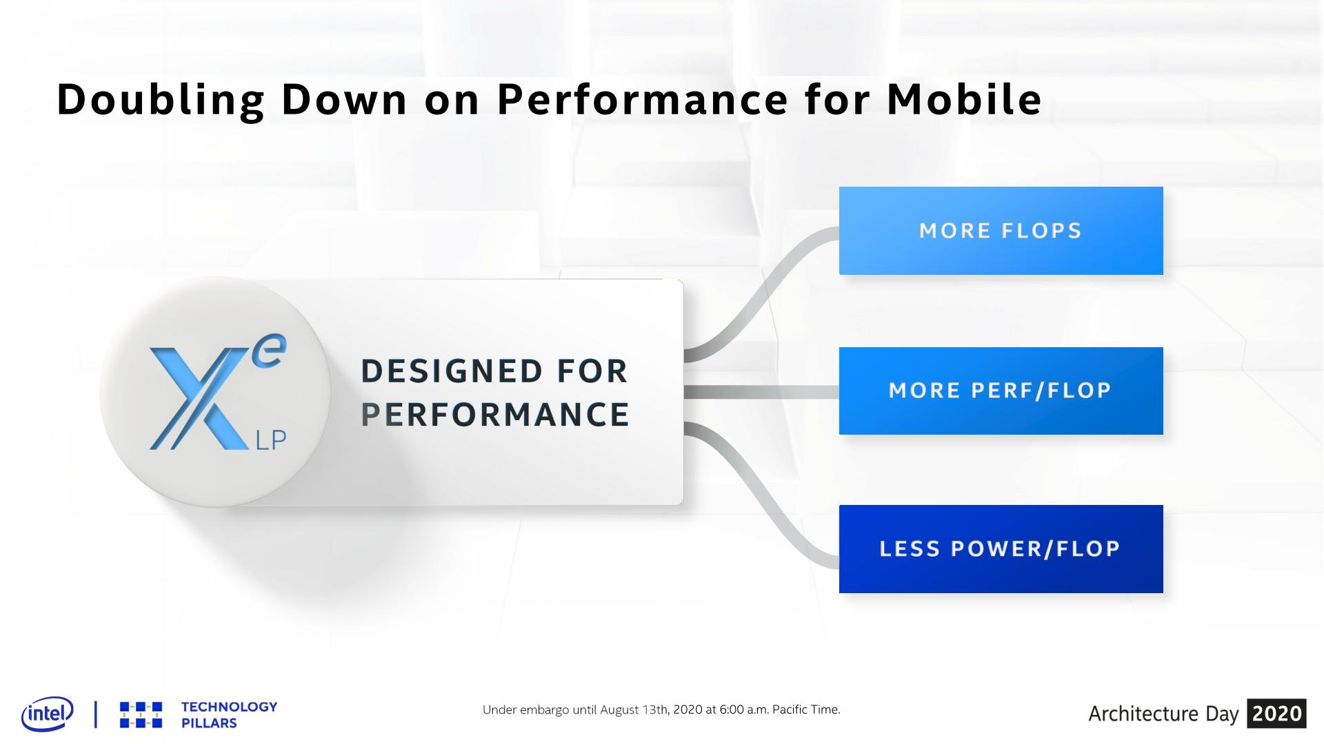
Rounding out Intel’s plan to boost GPU performance then comes from the third pillar of Xe-LP’s design, which is improving efficiency. While adding EUs adds FLOPs, and improving energy efficiency allows Intel to clock the chip higher to add even more FLOPs, adding FLOPs alone isn’t enough. Work must also go into improving the effective throughput of an architecture, to covert more of those theoretical FLOPs into real-world work.
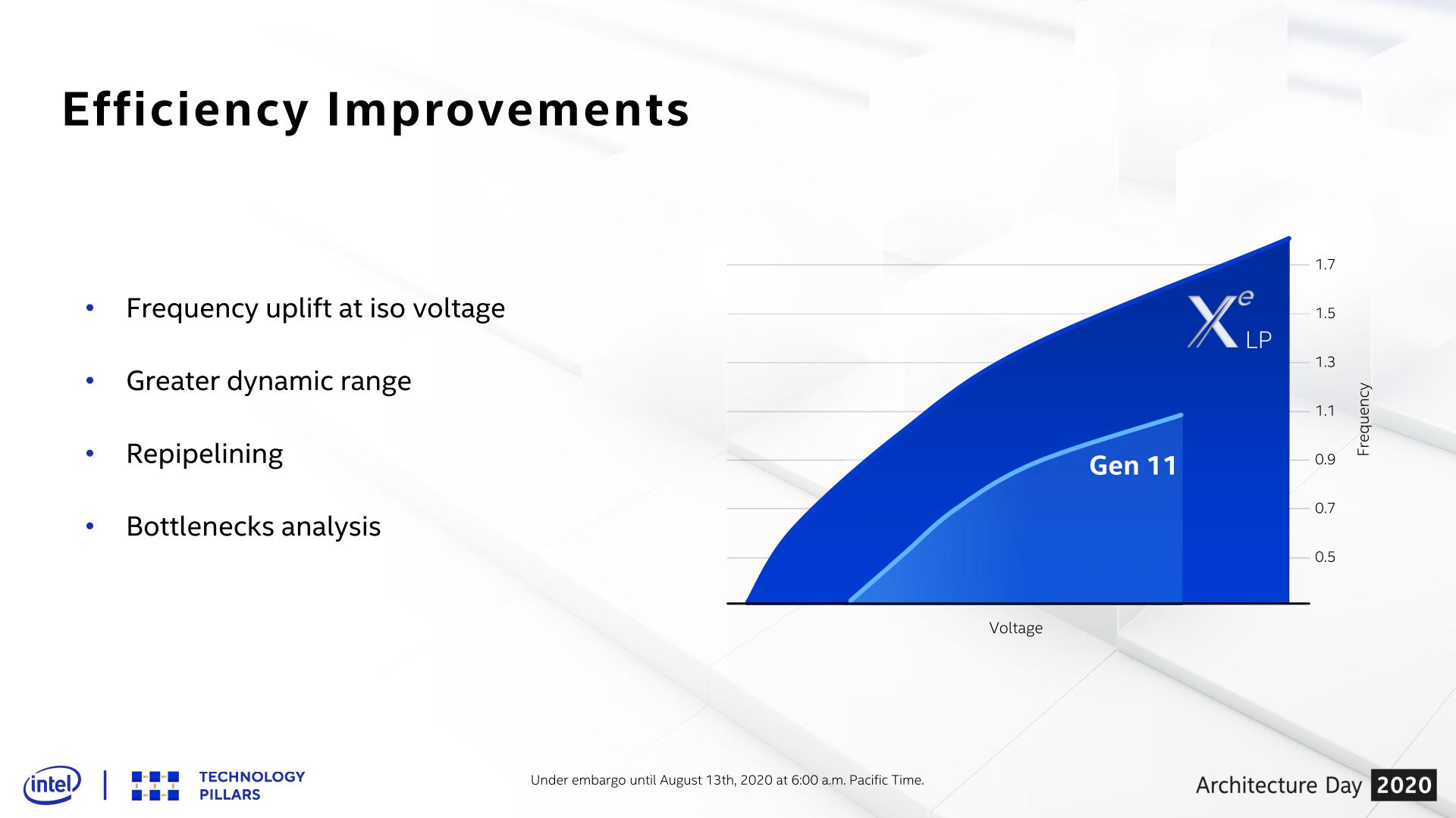
And this is where Intel’s secret sauce comes in, and not as much from Intel’s technical marketing department comes out. There are some notable low-level EU changes that we’ll get to in a moment, but these are more about driving the aforementioned power efficiency changes. Instead, the throughput efficiency changes are more opaque. Here Intel merely tells us that they’ve used workload analysis to identify and remove multiple small bottlenecks throughout the GPU to improve graphics and compute throughput efficiency.
Intel’s L1 cache changes likely also play a part here, though the company isn’t going too much into those changes at this time. None the less, we’ll catch up on the subject in a bit when looking at the overall memory system.
Subslice Reorganization
One further consequence of widening the overall slice is that Intel has reorganized the subslice within the larger slice. Analogous in a few ways to NVIDIA’s SMs, a subslice is a smaller building block within the GPU, focused on compute and shading in all forms, as well as texturing. For Intel’s Gen11 GPUs, the company organized the GPUs into 8 subslices, each containing 8 EUs. But with Xe-LP, each subslice has been bulked up, and the number of overall subslices has been reduced.
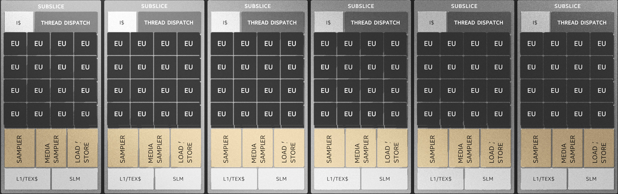
A full slice on Xe-LP is now 6 subslices. Each Xe-LP subslice, in turn, has seen many of its attributes doubled. The number of EUs in a subslice is doubled to 16 per, and the throughput of a subslice’s texture sampler has been bumped up from 4 texels/clock to 8 texels/clock. Each subslice also gets an L1 data/texture cache, which is 64KB and can be dynamically allocated between L1 data and texture storage. This cache would seem to replace Gen11’s poorly documented L2 cache, which occupied a similar role in the hierarchy.
These subslice changes, in turn, go hand-in-hand with some of the changes Intel made to the EUs, which we’ll cover on the next page. With EUs losing a little bit of their independence and getting paired off, this keeps the number of thread control units per subslice constant at 8. It’s likely to also help Intel’s scalability towards future solutions, as they have fewer subslices to wrangle and manage overall.
One consequence of this change means that Intel’s iGPU scalability steps will also be a bit different. Whereas Ice Lake shipped with 64 EUs (8 subslices), 48 EUs (6 subslices), or 32 EUs (4 subslices) enabled, depending on the SKU, Tiger Lake’s granularity is now one-sixth of a slice. So that means half of a GPU is now 48 EUs (3 subslices), a full GPU is 96 EUs (6 subslices), and Intel will have to decide if and how it wants to ship SKUs in the middle with 80 or 64 EUs enabled. As Intel isn’t providing production information today, we can only speculate, but it would be a pretty huge drop in performance if the next tier down after a fully-enabled Xe-LP iGPU was a 64 EU configuration, shedding 33% of its potential performance along the way.
Xe-LP Execution Units: It Takes Two
Diving down a level deeper, we have the smallest thread-level building block of the Xe-LP GPU architecture, the venerable Execution Unit. Intel has tweaked these a few times over the years, and for Xe-LP they are getting tweaked once again.
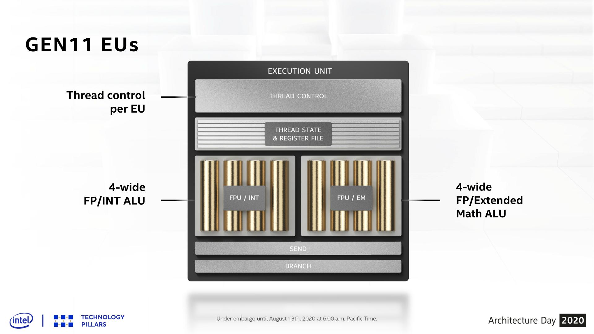
As a quick refresher, as of Intel’s Gen11 GPU architecture, an EU is comprised of a single thread control unit and two sets of 4-wide SIMDs. One block handles floating point and integer math, while the other block can handle floating point and special functions, which Intel refers to as “extended math”. Despite this, Gen11’s smallest wavefront width is 8 threads wide (SIMD8), so it can take multiple clock cycles to execute a single wavefront, with Intel interleaving multiple wavefronts as a form of latency hiding.
Xe-LP, meanwhile, brings several important changes to the design of the EUs. First and foremost, a single EU is no longer a stand-alone block; instead two EUs now share a single thread control unit. As a result, a thread control unit now gets the combined resource of two EUs to spread work over, instead of the one. And while the SIMD arrays themselves have also changed – further complicating matters – the impact here is that there are now fewer thread control units in a GPU, which should reduce the number of wavefronts that are in-flight at any given moment.
In fact there’s an argument to be had whether calling these dual EU setups two EUs is even the most accurate way to describe them; it might be better to instead bundle them together as a single fat EU, since neither half is truly independent. But absent further low-level details, and what I’m sure is a desire by Intel to be semi-consistent in counting EUs, they are going with 96 thin EUs.
Meanwhile regardless of how you bundle the EUs, there’s also the matter of what’s in the EUs themselves. For Xe-LP, Intel has reorganized the SIMD blocks. Gone are the pair of feature-differentiated SIMD4 blocks in favor of a SIMD8 block and a SIMD2 block. The larger SIMD8 essentially combines all of the floating point and integer ALUs that previously were split between Gen11’s two SIMD4 blocks, and makes a single SIMD8 out of them. The net result is that the number of FPU ALUs hasn’t changed – it’s still 8 ALUs per EU – however the number of pipes that can process integers has changed from 4 to 8. Meanwhile, although not made clear in Intel's slides, the number of ALUs that can process extended math is staying constant: Gen11 had two EM-capable pipes, and Xe-LP does as well.
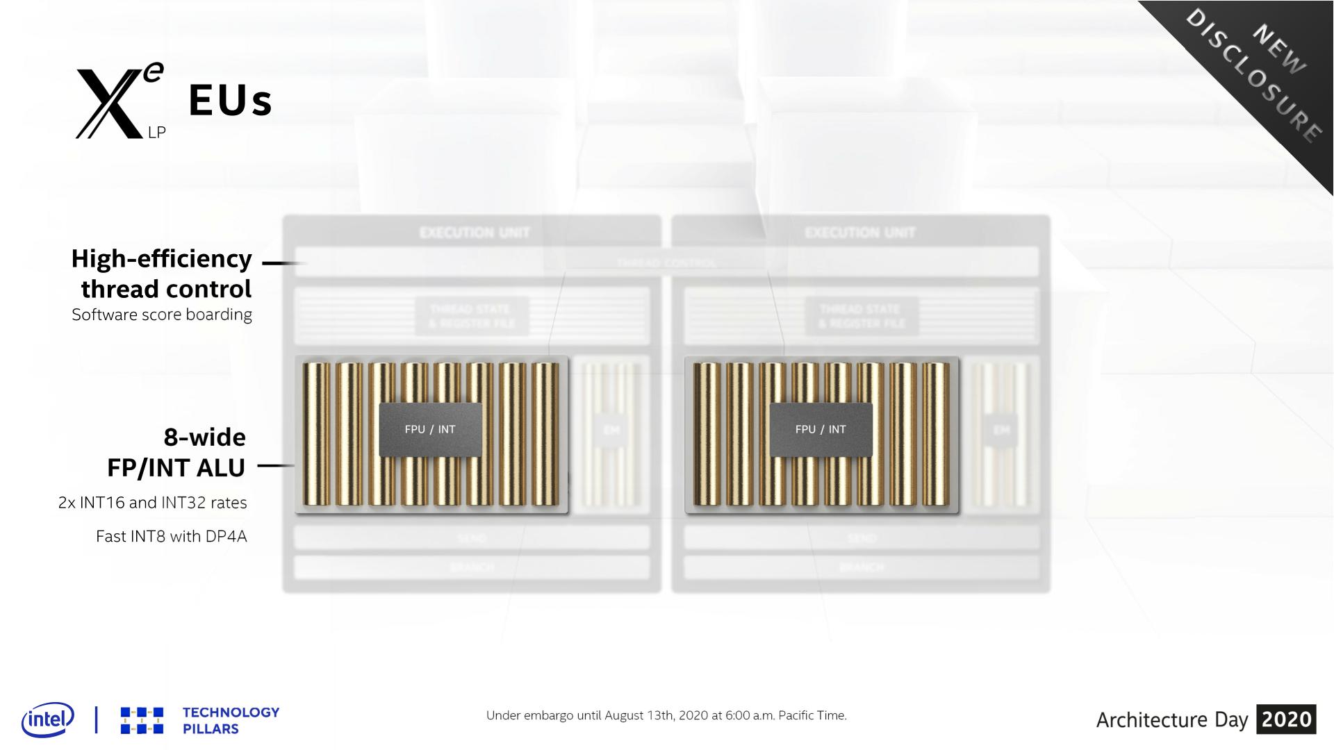
Speaking of which, extended math has now been moved to its own SIMD2, and every EU gets one. This means that executing extended math functions no longer directly blocks the execution of floating point arithmetic, as was the case for Gen11 – the EU doesn’t have to give up FP pipes to do this. Further underscoring this point, the EU can co-issue instructions to both the FP/INT SIMD8 and the EM SIMD2 at the same time, meaning that under at least some circumstances, doing extended math also won’t indirectly block FP/INT arithmetic.
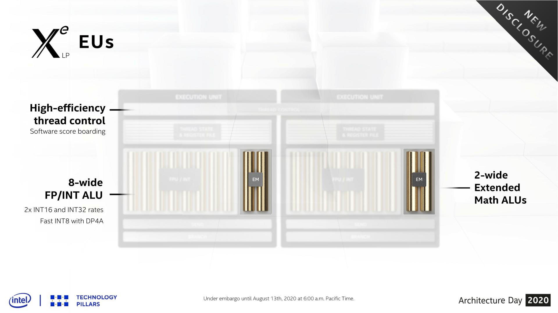
As always with co-issuing, the devil is in the details – at this point it’s not clear to us just what the co-issuing limitations are – but it’s still very likely to be a better fit to the kind of workloads Intel is actually seeing. AMD and NVIDIA also use dedicated EM/SFU units, and in similarly small ratios, all of which seems to work out well for those two companies. So in that respect Intel’s ALU setup is looking a lot more like its contemporary competitors’. And this, I suspect, is also one of the forms of bottleneck optimization that Intel has gone through to get more work out of the same number of FLOPs on Xe-LP.
These ALU changes also impact how wavefronts will move through the GPU. With a SIMD8 being the smallest ALU array for normal arithmetic, Intel’s minimum wavefront size is now the same size as the underlying hardware. This means that Xe-LP no longer needs multiple cycles to execute a single instruction from a wavefront in a single cycle, at least for the smallest wavefront size. In Gen11 Intel also allowed SIMD16 and SIMD32 wavefronts, and I’m waiting on the Xe-LP whitepaper to confirm whether those have been retained – in which case they’d still need multiple cycles – or if Intel is forcing everything to be SIMD8.
It’s worth noting that this change is fairly similar to what AMD did last year with its RDNA (1) architecture, eliminating the multi-cycle execution of a wavefront by increasing their SIMD size and returning their wavefront size. In AMD’s case this was done to help keep their SIMD slots occupied more often and reduce instruction latency, and I wouldn’t be surprised if it’s a similar story for Intel.

A further benefit of this reorganization is that Intel has been able to simplify their thread scheduling hardware overall. As recently as Gen11, Intel was still using hardware score boarding to determine when to run threads and when threads’ data would be ready. But with Xe-LP, score boarding has been moved into software, becoming a responsibility of Intel’s compiler.
While the move to software score boarding means that scheduling has to be determined in advance by the software – and thus becomes static and potentially results in less-than-optimal scheduling – the payoff is that hardware score boarding is fairly expensive from a die area and power standpoint. So moving to software score boarding allows for smaller and more power efficient EUs, which feeds back into Intel’s ability to build a larger number of EUs, and to improve their overall energy efficiency. Overall, this mirrors changes NVIDIA made to their architecture almost a decade ago with Kepler, where they similarly switched to software score boarding to the great benefit of their energy efficiency (and while retaining their high performance).
EU Throughput: By the Numbers
Now that we’ve had a chance to see all the changes made at the EU level, let’s talk about what this means for the actual throughput rates of the EUs.
| Intel GPU Compute Throughput Rates (FMA, Ops/clock/EU) |
||||
| Xe-LP | Gen11 | |||
| FP32 | 16 | 16 | ||
| FP16 | 32 | 32 | ||
| INT32 | 8 | 4 | ||
| INT16 | 32 | 16 | ||
| INT8 | 64 (DP4A) |
N/A | ||
Starting with floating point, things are simple here. Despite the ALU reorganization, the number of FP ALUs per EU is still 8. And as a result, FP throughput per EU remains at 16 FP32 ops/clock and 32 FP16 ops/clock, just like Gen11.
For integer throughput on the other hand, the number of integer-capable ALUs has been doubled from 4 to 8 relative to the Gen11 architecture. As a result, integer throughput has also doubled: Xe-LP can put away 8 INT32 ops or 32 INT16 ops per clock cycle, up from 4 and 16 respectively on Gen11. This does mean, however, that Xe-LP retains Gen11’s unusual INT32 handicap; the INT32 rate is only half the FP32 rate, whereas the INT16 rate is equal to the FP16 rate.
Finally, it’s worth nothing that Xe-LP doesn’t have anything equivalent to a tensor core or other systolic array of ALUs for doing dense math, which has become all the rage for neural networking training an inference. This hardware will be coming to the Xe family in later parts as the Xe Matrix eXtensions (XMX), but for now Xe-LP has to make do with its regular EUs.
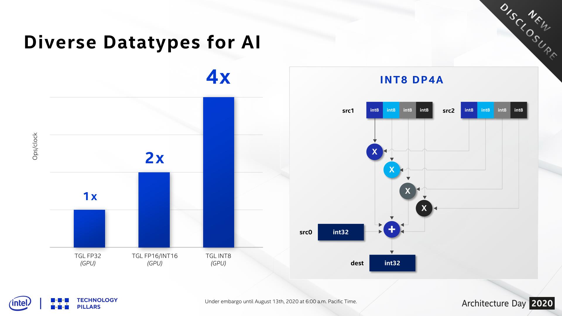
But for that reason, Intel has added one more feature to their EU SIMD: support for INT8 dot products. INT8 has become increasingly popular for neural networking inference over the past few years, and dot products in turn a very common operation in that process. So adding support for INT8 dot products gives Xe-LP a big boost in this form of AI execution. With the DP4A instruction, the INT8 throughput rate can get as high as 64 ops/clock, twice the INT16 rate.
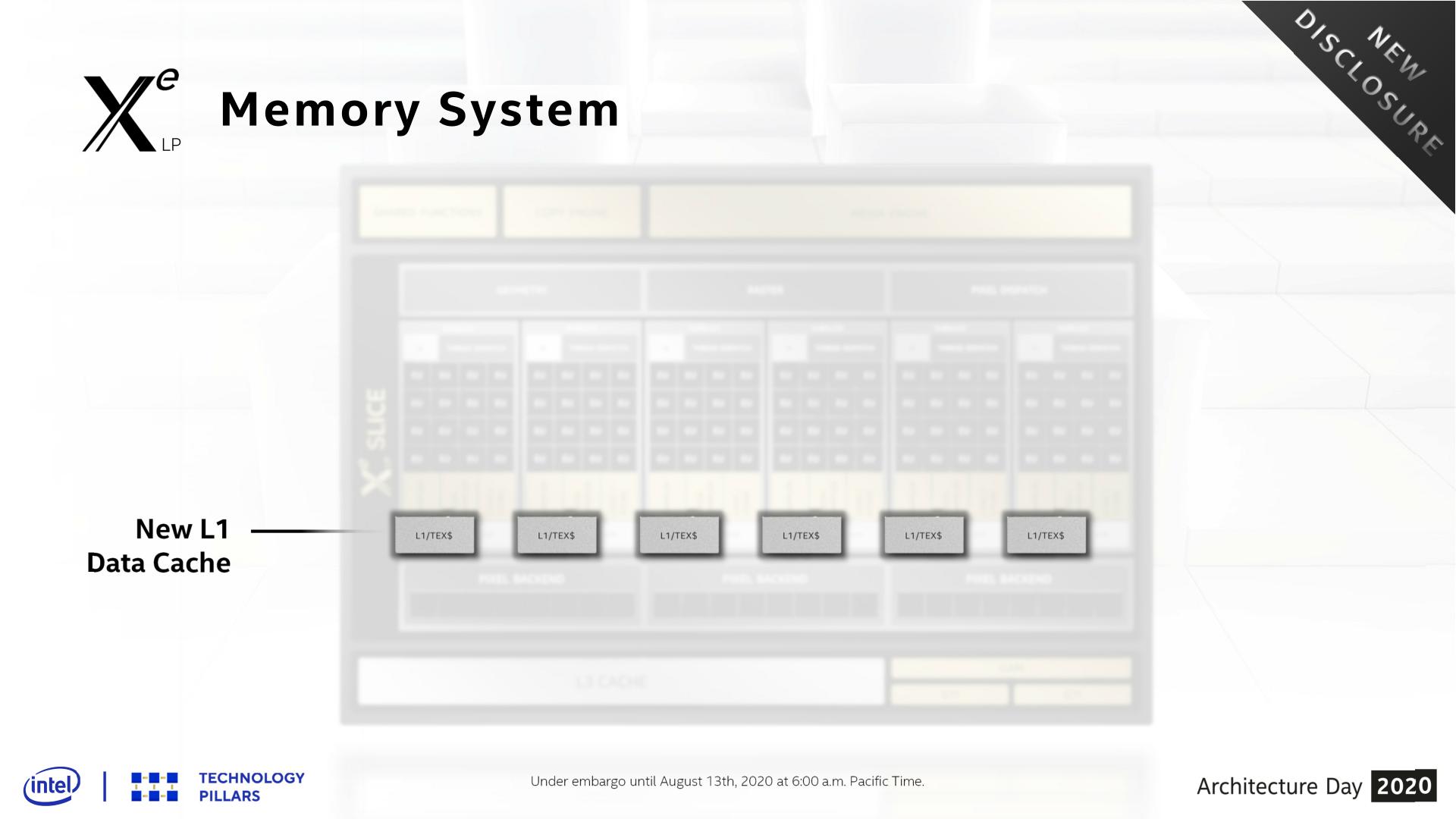
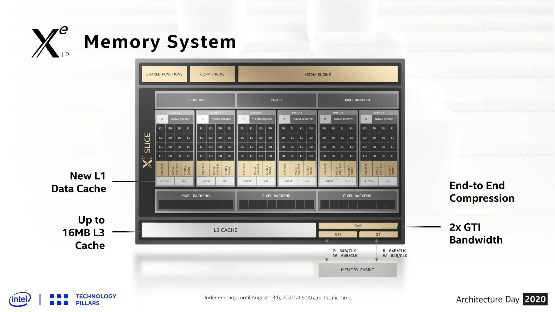
Feed the Beast: New L1 Cache & Dual Ring Buses
Shifting gears, let’s take a look at the memory subsystem for Xe-LP and how Intel will be feeding the beast that is their new GPU architecture. Among many contemporary firsts for Intel’s GPU architectures, Xe-LP will find itself in the interesting position of straddling the line between an integrated GPU and a discrete GPU. Which is to say that it has to be able to work with both Tiger Lake’s shared IMC, as well as DG1’s own dedicated memory controller.
Starting with the subslices, Xe-LP introduces a new combined L1 data and texture cache. Information about this cache is limited, but Intel has confirmed that it’s a 64KB per subslice cache, and that it can be dynamically reconfigured between L1 and texture caching as necessary. According to the company, they added the L1 cache as a result of their workload analysis, and that doing so improved the performance of the load/store pipeline. Unfortunately, it’s not clear how this fits into the bigger picture with Intel’s previous subslice L2 cache, and whether that’s been replaced or still exists and is merely not on these diagrams.
The on-GPU L3 cache (not to be confused with Tiger Lake’s shared Last Level Cache) has also undergone its own upgrades, receiving both a capacity and a bandwidth boost. On the capacity front, the L3 cache can now be as large as 16MB, as opposed to just 3MB on Gen11. That said, based on Intel’s Tiger Lake disclosures, it’s clear that such a large cache isn’t coming to Intel’s SoCs; instead Tiger Lake will ship with a 3.8MB GPU L3 cache. Tiger Lake has its own LLC beyond this, which the GPU can tap into as well, so it doesn’t necessarily need quite such a large cache.
For DG1, on the other hand, the GPU’s L3 cache is the last caching level, so a larger cache makes practical sense there. To that end I wouldn’t be surprised if that’s exactly what we see on DG1: a 16MB L3 cache. Though Intel has reiterated that this is an architectural presentation and not a product presentation, so it may very well be that they aren’t outfitting any Xe-LP GPUs with a max size L3 cache.
This larger L3 cache is also faster than Gen11’s L3, with Intel doubling the transfer size. Xe-LP’s L3 cache can now transfer 128 bytes/clock, which for a theoretical 1.6GHz chip would give it over 190GB/sec of internal L3 bandwidth. This upgrade is important for feeding the ROPs and other parts of the GPU, and goes hand-in-hand with Intel’s goal to double GPU performance, which means they need to feed the beast a lot more data in the process. Plus this change also keeps the L3 cache aligned with what the new dual ringbus can do.
One of the more enigmatic changes for Tiger Lake, the SoC has added a second, seemingly identical ringbus to the chip, creating a second loop that connects the four CPU cores and the iGPU to the integrated memory controller. As a consequence of this, the iGPU now needs two Graphics Technology Interface (GTI) ports to create the two ringbus stops.
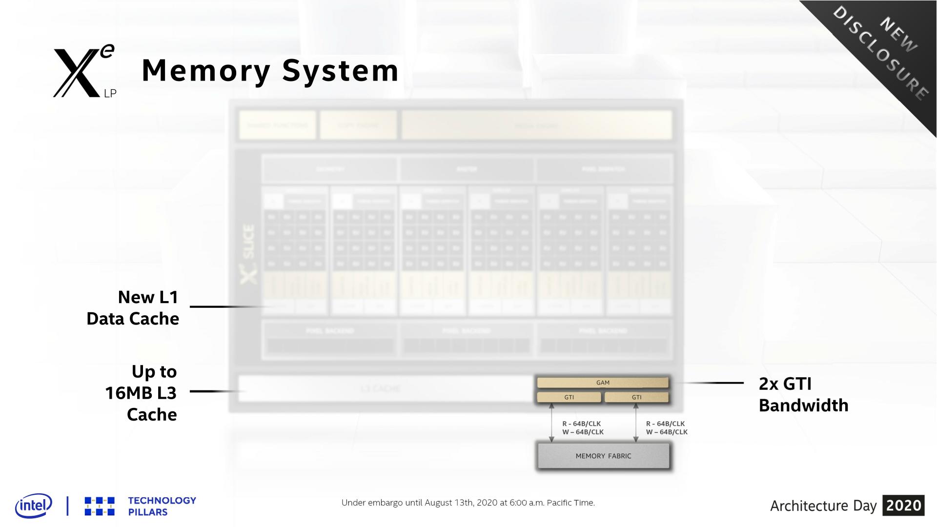
The big benefit of this change is that, all other aspects held equal, this doubles the amount of bandwidth between the GPU and the IMC on Tiger Lake. So instead of only being able to transfer 64B/clock up and down, Xe-LP on Tiger Lake can send two 64B requests (for a total of 128B/clock) using the two ringbuses.
Given that at this juncture the iGPU has become the largest consumer of bandwidth on an Intel SoC, I strongly suspect that the second ringbus has been added primarily for the iGPU’s benefit. Unfortunately this isn’t something we can directly math out, as the ringbus having its own clock domain complicates matters a bit, so it’s not clear if 1 ringbus can even match the memory bandwidth of a Tiger Lake chip with LPDDR5-5200. But even if it can, the an even higher performing GPU like Xe-LP is no doubt putting a good deal of pressure on Intel’s SoC memory subsystem.
Meanwhile this also gives us a very strong hint that DG1 will utilize a 128-bit memory bus for its dedicated VRAM. The 2x64B backend could very easily be hooked up to a 128-bit memory controller, instead of the two 64B ringbuses. This would also ensure that DG1 gets as much or more memory bandwidth than Tiger Lake – and with the bonus of not having to share it with other parts of the system.
Finally, even with the significant bandwidth improvements underneath, Intel has also been working to reduce their bandwidth consumption. Xe-LP ships with updated versions of their color and depth compression algorithms, which although Intel isn’t providing specific figures for it, any improvements here will directly translate into reduced memory traffic. Meanwhile the company is also extending this compression functionality to the media and display interfaces, which means that image data can stay compressed whenever it’s being moved between the graphics engine, the media engine, and the display.
Xe-LP Media & Display Controllers
Our final stop on our deep dive through the Xe-LP architecture are the non-rendering aspects of the GPU: its media and display controllers. Changes here aren’t quite as eye-catching as changes to the core architecture, but the improvements made in these blocks help to keep the overall GPU current by supporting new media formats as well as new display connectivity protocols.
First off, let’s talk about the media engine. There are no crazy overhauls to speak of here, but for Xe-LP Intel has made some sensible additions to the engine. The marquee feature here is easily support for AV1 decode acceleration, making Intel the first vendor out of the Big 3 to add hardware decode support for the new codec.
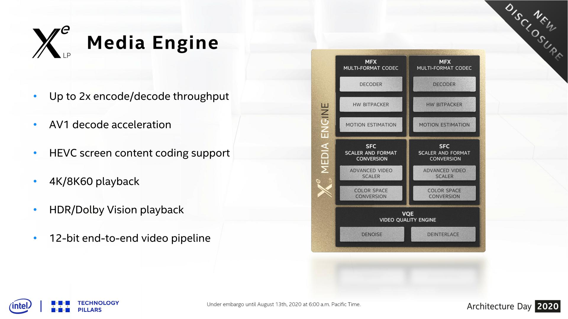
The up-and-coming royalty free codec is widely expected to become the de facto successor to H.264/AVC, as while HEVC has been on the market for a number of years (and is already supported in all recent GPUs), the madcap royalty situation around the codec has discouraged its adoption. By contrast, AV1 should deliver similar or slightly better quality than HEVC without royalties for its use in distribution, which makes it a lot more palatable to content vendors. The one downside to AV1 thus far is that it’s pretty CPU heavy, which makes hardware decode support all the more important not only for battery life reasons, but even ensuring smooth, glitch-free playback.
Meanwhile, similar to Intel’s rendering performance goals, the company has worked to improve the encoding and decoding throughput of the media engine. According to the company the updated block is now capable of up to 2x the encode and decode throughput. For consumer machines this is unlikely to matter too much, but it’s something that will be particularly important for the SG1 server product, which will focus on bulk encoding.
Finally, among smaller changes made to the media engine, Intel has added official support for HDR and Dolby Vision playback. HDR support continues to roll out to PCs, if only slowly, so this is a notable step in ensuring that newer PCs can handle HDR content encoded in those formats. Also notable is an improvement to Intel’s HEVC encoding block, which now supports the HEVC Screen Content Coding (SCC) extension, which is designed to improve HEVC compression rates on content with static or nearly-static images.
Xe-LP Display Controller: DisplayPort 1.4, HDMI 2.0, & 8K Displays
Last but certainly not least, we have Xe-LP’s display engine. Like the media block there are no radical changes here, but there are some welcome improvements throughout.
Perhaps the biggest change here is that after several years, Intel has finally added a fourth display pipeline, meaning that the GPU can now drive four independent displays. Prior to this, Gen11 and earlier designs could only handle three displays, and though even that is more than most people will use, 4 displays has become the magic number for other GPU designs. Complicating matters is the recent push for dual screen laptops and other mobile devices with multiple displays, which would then eat up two of those three outputs.
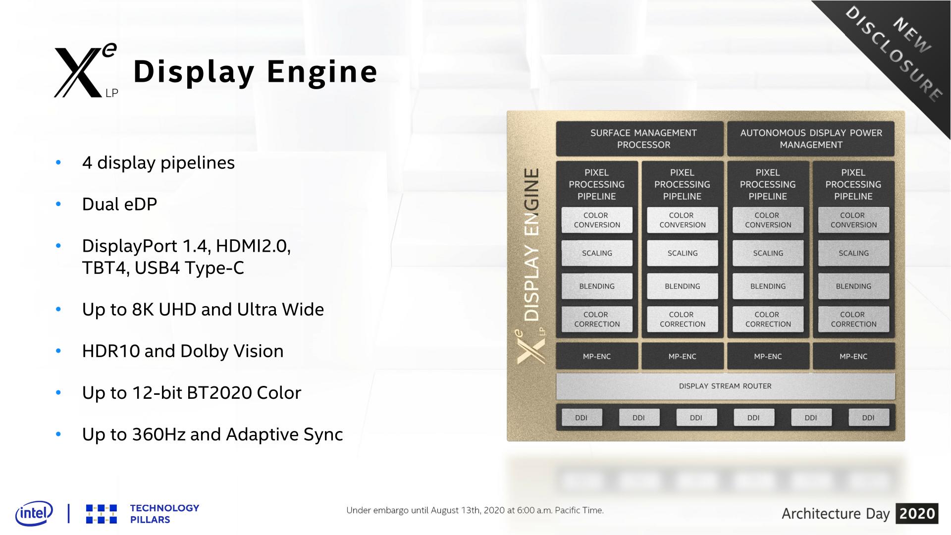
On which note, Intel has also added a second embedded DisplayPort output, which would be extremely useful for those dual screen devices.
Otherwise, the basic display output choices are unchanged from Gen11. Xe-LP supports DisplayPort 1.4 as well as HDMI 2.0. The latter is a bit disappointing since HDMI 2.1 televisions are now shipping, but it’s admittedly not unusual for Intel to take an extra generation to adopt newer HDMI standards. These display outputs can also be fed into a USB4/Thunderbolt 4 port, where DisplayPort data is a first-class citizen and can be muxed in the signal, or the port reconfigured via alt modes.
Not evident on Intel’s block diagrams, the company has made some plumbing changes to better feed the display controllers. Specifically, the company has increased the bandwidth available to the display engine so that it can handle the kind of extreme, high-resolution displays that DisplayPort 1.4 was designed to feed. As a result the controller now has enough bandwidth and internal processing power to drive 8K UHD displays, as well as the recent generation of 360Hz displays.
Performance Expectations & First Thoughts
Wrapping up this GPU architecture deep dive, while Intel didn’t use this year’s architecture day to discuss specific products and SKUs, the company did take a moment to discuss performance expectations for Xe-LP, and offer some quick videos of Xe-LP in action. Unfortunately we weren’t allowed to record these demos (least someone leak them), but we’ll post them here as soon as Intel releases copies to the public.

At any rate, as previously discussed, Intel’s goal was to double Ice Lake’s (Gen11) graphics performance, which Xe-LP will be accomplishing via a combination of a wider GPU (more hardware), a more power-efficient GPU (allowing higher clocks), and a more throughput-efficient GPU (higher IPC). This is a lofty goal given the fact that they don’t get the benefit of a wholly new process node, but Intel does seem rather confident about the performance potential of its new 10nm SuperFin process node, as well as the payoff from the tried-and-true method of brute forcing things by throwing more hardware at it.
Looking at our own performance data from reviews of Ice Lake and Ryzen 3000 “Renoir” laptops, if Intel can meet their performance goals then Tiger Lake should be able to pull ahead of AMD’s comparable U-series Ryzen APUs. As always, this is going to be game-dependent, but high-end Ice Lake laptops were never behind by more than 30% or so in GPU-limited scenarios. But since we’re talking about mobile scenarios, the power and cooling will always be a potential wildcard that can hold a laptop back. So for ultraportable gaming laptops in particular, Intel will undoubtedly want its partners to build laptops with the cooling capabilities to match, to give Tiger Lake every possible chance to succeed.
Framerates aside, Intel also expects Xe-LP’s performance to significantly raise the bar on image quality. With integrated graphics generally bringing up the rear in terms of image quality in order to deliver the necessary framerates, doubling their iGPU performance would allow a lot of games to be run at higher image quality settings. This again would vary from game to game, but at least for promotional purposes, Intel is eyeballing Tiger Lake/Xe-LP being able to run at high image quality in games where Ice Lake could only manage low.
But Xe-LP isn’t just an integrated graphics solution: it’s for discrete graphics too. And while we eagerly anticipate more information on DG1, given Intel’s focus today on architecture over products, we’re left with more questions than answers. Intel has a very interesting and OEM-friendly plan in place with Xe-LP, and by leveraging the same architecture for both the iGPU and an optional discrete GPU, OEMs are going to love the fact that they don’t have to validate and load separate GPU drivers for the integrated and discrete GPUs.
Most importantly, however, Intel is also refusing to answer the 10 million pixel question: will Tiger Lake’s iGPU be able to work in concert with the DG1? Intel has certainly not made any efforts to shoot down that idea, but they also aren’t confirming it, either. And even then, if they utilize mutli-GPU rendering, will they get it right? Multi-GPU rendering on the desktop is all but dead, and for good reason: it tends not to play nicely with certain modern rendering techniques, and it can add a fair bit of input lag. The answer to this question – and whether Intel has been able to conquer the traditional drawbacks of multi-GPU rendering – will absolutely have a huge impact on the commercial viability of the DG1 GPU. So we’ll be eagerly awaiting the answer to those questions.
Otherwise, Xe-LP marks an important step in the evolution of Intel’s GPU architectures, never mind a huge stepping stone in their plans to become a top-to-bottom GPU supplier. Though only destined for laptops, Xe-LP is the basis of something much bigger for Intel: Xe-LP will be the foundation of an entire generation of GPUs to come. So what Intel does here with regards to features, architecture, and above all else power efficiency will have enormous repercussions to come, for everything from gaming hardware to supercomputers. In many ways it’s the dawn of a new era for Intel, and one they are hoping will be a better era than what they leave behind.


